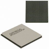
EP3SL150F1152C3N Altera, EP3SL150F1152C3N Datasheet - Page 410

EP3SL150F1152C3N
Manufacturer Part Number
EP3SL150F1152C3N
Description
IC STRATX III FPGA 150K 1152FBGA
Manufacturer
Altera
Series
Stratix® IIIr
Datasheets
1.EP3SL150F780C4N.pdf
(16 pages)
2.EP3SL150F780C4N.pdf
(332 pages)
3.EP3SL150F780C4N.pdf
(456 pages)
Specifications of EP3SL150F1152C3N
Number Of Logic Elements/cells
142500
Number Of Labs/clbs
5700
Total Ram Bits
6390
Number Of I /o
744
Voltage - Supply
0.86 V ~ 1.15 V
Mounting Type
Surface Mount
Operating Temperature
0°C ~ 85°C
Package / Case
1152-FBGA
For Use With
544-2568 - KIT DEVELOPMENT STRATIX III
Lead Free Status / RoHS Status
Lead free / RoHS Compliant
Number Of Gates
-
Other names
544-2408
EP3SL150F1152C3NES
EP3SL150F1152C3NES
Available stocks
Company
Part Number
Manufacturer
Quantity
Price
Company:
Part Number:
EP3SL150F1152C3N
Manufacturer:
ALTERA
Quantity:
490
- Current page: 410 of 456
- Download datasheet (7Mb)
13–12
Figure 13–9. SAMPLE/PRELOAD Shift Data Register Waveforms
Note to
(1) Data stored in boundary-scan register is shifted out of TDO.
(2) After boundary-scan register data has been shifted out, data entered into TDI will shift out of TDO.
Stratix III Device Handbook, Volume 1
Figure
TAP_STATE
TMS
TDO
TCK
TDI
13–9:
SHIFT_IR
Instruction Code
During the capture phase, multiplexers preceding the capture registers select the
active device data signals. This data is then clocked into the capture registers. The
multiplexers at the outputs of the update registers also select active device data to
prevent functional interruptions to the device. During the shift phase, the
boundary-scan shift register is formed by clocking data through the capture registers
around the device periphery and then out of the TDO pin. The device can
simultaneously shift new test data into TDI and replace the contents of the capture
registers. During the update phase, data in the capture registers is transferred to the
update registers. You can then use this data in the EXTEST instruction mode. Refer to
“EXTEST Instruction Mode” on page 13–13
Figure 13–9
instruction code is shifted in through the TDI pin. The TAP controller advances to the
CAPTURE_DR state and then to the SHIFT_DR state, where it remains if TMS is held
low. The data that was present in the capture registers after the capture phase is
shifted out of the TDO pin. New test data shifted into the TDI pin appears at the TDO
pin after being clocked through the entire boundary-scan register. If TMS is held high
on two consecutive TCK clock cycles, the TAP controller advances to the UPDATE_DR
state for the update phase.
EXIT1_IR
shows the SAMPLE/PRELOAD waveforms. The SAMPLE/PRELOAD
UPDATE_IR
SELECT_DR
CAPTURE_DR
Chapter 13: IEEE 1149.1 (JTAG) Boundary-Scan Testing in Stratix III Devices
(1)
for more information.
IEEE Std. 1149.1 BST Operation Control
SHIFT_DR
© July 2010 Altera Corporation
(2)
UPDATE_DR
EXIT1_DR
Related parts for EP3SL150F1152C3N
Image
Part Number
Description
Manufacturer
Datasheet
Request
R

Part Number:
Description:
CYCLONE II STARTER KIT EP2C20N
Manufacturer:
Altera
Datasheet:

Part Number:
Description:
CPLD, EP610 Family, ECMOS Process, 300 Gates, 16 Macro Cells, 16 Reg., 16 User I/Os, 5V Supply, 35 Speed Grade, 24DIP
Manufacturer:
Altera Corporation
Datasheet:

Part Number:
Description:
CPLD, EP610 Family, ECMOS Process, 300 Gates, 16 Macro Cells, 16 Reg., 16 User I/Os, 5V Supply, 15 Speed Grade, 24DIP
Manufacturer:
Altera Corporation
Datasheet:

Part Number:
Description:
Manufacturer:
Altera Corporation
Datasheet:

Part Number:
Description:
CPLD, EP610 Family, ECMOS Process, 300 Gates, 16 Macro Cells, 16 Reg., 16 User I/Os, 5V Supply, 30 Speed Grade, 24DIP
Manufacturer:
Altera Corporation
Datasheet:

Part Number:
Description:
High-performance, low-power erasable programmable logic devices with 8 macrocells, 10ns
Manufacturer:
Altera Corporation
Datasheet:

Part Number:
Description:
High-performance, low-power erasable programmable logic devices with 8 macrocells, 7ns
Manufacturer:
Altera Corporation
Datasheet:

Part Number:
Description:
Classic EPLD
Manufacturer:
Altera Corporation
Datasheet:

Part Number:
Description:
High-performance, low-power erasable programmable logic devices with 8 macrocells, 10ns
Manufacturer:
Altera Corporation
Datasheet:

Part Number:
Description:
Manufacturer:
Altera Corporation
Datasheet:

Part Number:
Description:
Manufacturer:
Altera Corporation
Datasheet:

Part Number:
Description:
Manufacturer:
Altera Corporation
Datasheet:

Part Number:
Description:
CPLD, EP610 Family, ECMOS Process, 300 Gates, 16 Macro Cells, 16 Reg., 16 User I/Os, 5V Supply, 25 Speed Grade, 24DIP
Manufacturer:
Altera Corporation
Datasheet:


