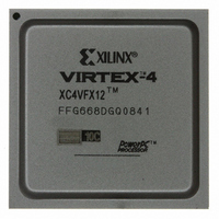
XC4VFX12-10FFG668C Xilinx Inc, XC4VFX12-10FFG668C Datasheet - Page 19

XC4VFX12-10FFG668C
Manufacturer Part Number
XC4VFX12-10FFG668C
Description
IC FPGA VIRTEX-4 FX 12K 668FCBGA
Manufacturer
Xilinx Inc
Series
Virtex™-4r
Datasheets
1.XC4VFX12-10FFG668C.pdf
(58 pages)
2.XC4VFX12-10FFG668C.pdf
(9 pages)
3.XC4VFX12-10FFG668C.pdf
(406 pages)
Specifications of XC4VFX12-10FFG668C
Total Ram Bits
663552
Number Of Logic Elements/cells
12312
Number Of Labs/clbs
1368
Number Of I /o
320
Voltage - Supply
1.14 V ~ 1.26 V
Mounting Type
Surface Mount
Operating Temperature
-40°C ~ 100°C
Package / Case
668-BBGA, FCBGA
No. Of Logic Blocks
12312
No. Of Macrocells
12312
No. Of Speed Grades
10
No. Of I/o's
320
Clock Management
DCM
I/o Supply Voltage
3.45V
Lead Free Status / RoHS Status
Lead free / RoHS Compliant
For Use With
HW-V4-ML403-UNI-G - EVALUATION PLATFORM VIRTEX-4HW-AFX-FF668-400 - BOARD DEV VIRTEX 4 FF668
Number Of Gates
-
Lead Free Status / RoHS Status
Lead free / RoHS Compliant, Lead free / RoHS Compliant
Other names
122-1591
XC4VFX12-10FFG668C
XC4VFX12-10FFG668C
Available stocks
Company
Part Number
Manufacturer
Quantity
Price
Company:
Part Number:
XC4VFX12-10FFG668C
Manufacturer:
Xilinx Inc
Quantity:
10 000
IOB Pad Input/Output/3-State Switching Characteristics
Table 27
input delay adjustments, output delays terminating at pads
(based on standard and 3-state delays.
T
input buffer to the I-pin of an IOB pad. The delay varies
depending on the capability of the SelectIO input buffer.
T
pad through the output buffer of an IOB pad. The delay var-
ies depending on the capability of the SelectIO output
buffer.
Table 27: IOB Switching Characteristics
DS302 (v3.7) September 9, 2009
Product Specification
LVDS_25
RSDS_25
LVDSEXT_25
LDT_25
BLVDS_25
ULVDS_25
PCI33_3
(PCI, 33 MHz, 3.3V)
PCI66_3
(PCI, 66 MHz, 3.3V)
PCI-X
GTL
GTLP
HSTL_I
HSTL_II
HSTL_III
HSTL_IV
HSTL_I _18
HSTL_II _18
HSTL_III _18
HSTL_IV_18
SSTL2_I
SSTL2_II
LVTTL, Slow, 2 mA
LVTTL, Slow, 4 mA
LVTTL, Slow, 6 mA
LVTTL, Slow, 8 mA
IOPI
IOOP
is described as the delay from IOB pad through the
is described as the delay from the O pin to the IOB
IOSTANDARD
Attribute
summarizes the values of standard-specific data
(1)
1.00
1.00
1.01
1.00
1.00
1.00
0.76
0.76
0.76
1.28
1.31
1.28
1.28
1.28
1.28
1.26
1.26
1.26
1.26
1.31
1.31
0.76
0.76
0.76
0.76
-12
Speed Grade
T
1.15
1.15
1.16
1.15
1.15
1.15
0.87
0.87
0.87
1.47
1.51
1.47
1.47
1.47
1.47
1.44
1.44
1.44
1.44
1.51
1.51
0.87
0.87
0.87
0.87
-11
IOPI
(1,2)
1.28
1.28
1.30
1.28
1.28
1.28
0.97
0.97
0.97
1.63
1.68
1.64
1.64
1.64
1.64
1.60
1.60
1.60
1.60
1.68
1.68
0.97
0.97
0.97
0.97
-10
www.xilinx.com
Virtex-4 FPGA Data Sheet: DC and Switching Characteristics
1.61
1.61
1.65
1.58
1.99
1.59
2.52
2.22
2.19
1.75
1.75
2.00
1.83
1.90
1.75
1.89
1.85
1.80
1.77
2.06
1.85
5.66
4.10
4.00
4.00
-12
T
pad through the output buffer of an IOB pad, when 3-state is
disabled. The delay varies depending on the SelectIO capa-
bility of the output buffer.
Table 28
described as the delay from the T pin to the IOB pad
through the output buffer of an IOB pad, when 3-state is
enabled (i.e., a high impedance state).
IOTP
Speed Grade
T
is described as the delay from the T pin to the IOB
1.71
1.71
1.75
1.68
2.15
1.68
2.76
2.46
2.21
1.87
1.87
2.16
1.96
2.04
1.87
2.03
1.98
1.93
1.89
2.23
1.98
6.37
4.57
4.46
4.46
-11
IOOP
summarizes the value of T
1.85
1.85
1.91
1.82
2.34
1.83
3.02
2.72
2.25
2.03
2.03
2.35
2.13
2.22
2.03
2.21
2.16
2.09
2.06
2.43
2.16
7.03
5.04
4.91
4.91
-10
1.61
1.61
1.65
1.58
1.99
1.59
2.52
2.22
2.19
1.75
1.75
2.00
1.83
1.90
1.75
1.89
1.85
1.80
1.77
2.06
1.85
5.66
4.10
4.00
4.00
-12
Speed Grade
T
1.71
1.71
1.75
1.68
2.15
1.68
2.76
2.46
2.21
1.87
1.87
2.16
1.96
2.04
1.87
2.03
1.98
1.93
1.89
2.23
1.98
6.37
4.57
4.46
4.46
-11
IOTP
IOTPHZ
1.85
1.85
1.91
1.82
2.34
1.83
3.02
2.72
2.25
2.03
2.03
2.35
2.13
2.22
2.03
2.21
2.16
2.09
2.06
2.43
2.16
7.03
5.04
4.91
4.91
-10
. T
IOTPHZ
Units
ns
ns
ns
ns
ns
ns
ns
ns
ns
ns
ns
ns
ns
ns
ns
ns
ns
ns
ns
ns
ns
ns
ns
ns
ns
19
is


