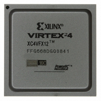
XC4VFX12-10FFG668C Xilinx Inc, XC4VFX12-10FFG668C Datasheet - Page 55

XC4VFX12-10FFG668C
Manufacturer Part Number
XC4VFX12-10FFG668C
Description
IC FPGA VIRTEX-4 FX 12K 668FCBGA
Manufacturer
Xilinx Inc
Series
Virtex™-4r
Datasheets
1.XC4VFX12-10FFG668C.pdf
(58 pages)
2.XC4VFX12-10FFG668C.pdf
(9 pages)
3.XC4VFX12-10FFG668C.pdf
(406 pages)
Specifications of XC4VFX12-10FFG668C
Total Ram Bits
663552
Number Of Logic Elements/cells
12312
Number Of Labs/clbs
1368
Number Of I /o
320
Voltage - Supply
1.14 V ~ 1.26 V
Mounting Type
Surface Mount
Operating Temperature
-40°C ~ 100°C
Package / Case
668-BBGA, FCBGA
No. Of Logic Blocks
12312
No. Of Macrocells
12312
No. Of Speed Grades
10
No. Of I/o's
320
Clock Management
DCM
I/o Supply Voltage
3.45V
Lead Free Status / RoHS Status
Lead free / RoHS Compliant
For Use With
HW-V4-ML403-UNI-G - EVALUATION PLATFORM VIRTEX-4HW-AFX-FF668-400 - BOARD DEV VIRTEX 4 FF668
Number Of Gates
-
Lead Free Status / RoHS Status
Lead free / RoHS Compliant, Lead free / RoHS Compliant
Other names
122-1591
XC4VFX12-10FFG668C
XC4VFX12-10FFG668C
Available stocks
Company
Part Number
Manufacturer
Quantity
Price
Company:
Part Number:
XC4VFX12-10FFG668C
Manufacturer:
Xilinx Inc
Quantity:
10 000
DS302 (v3.7) September 9, 2009
Product Specification
09/07/06
10/06/06
12/11/06
Date
Version
1.16
1.17
2.0
•
•
•
•
•
•
•
•
•
•
•
•
•
•
•
•
•
•
•
•
•
•
•
•
•
•
Added 2.5V rows to V
110 mV in
Table
T
IDELAYTOTAL_ERR
SPEED SPECIFICATION version for this data sheet release: v1.62.
Table
Table
devices to Production status.
Table
when APU Not Used and Characteristics when APU Used. Removed specs for
CPMFCMCLK, not available.
Table
Table
v1.62 speed specification.
SPEED SPECIFICATION version for this data sheet release: v1.62.
Table
parameters.
Table
Table
Table
622 MHz. Added DDR2 SDRAM (High-Performance SERDES Design) with reference
to XAPP721. Updated all specification values.
Pin-to-Pin Performance and Register-to-Register Performance tables (formerly Table
13 and Table 14) deleted.
Table
Table
Table
Table
respectively.
Table
setup/hold parameters relative to C, not CLKDIV.
Table
Table
characteristics. Changed T
Analyzer. Modified formula for T
Table
parameter.
Table
grade.
Table
Table
also apply to DLL and DFS together.
Table
DLL parameters.
Table
Table
Added Note (2) to indicate that PMCD outputs introduce no jitter.
14. Updated jitter tolerance and V
1: Removed former note 3 on V
14: Moved XC4VFX12-11, XC4VFX20-11, XC4VFX60-11, and XC4VFX100-11
15: Expanded to break out processor clock specifications into Characteristics
25,
39: Modified T
1: Modified Note (3) referring to 3.3V I/O design guidelines. Added I
2: Corrected recommended V
7: Added LVDCI attributes with LVCMOS.
13: Added Note (1) for SDR LVDS Interface requiring AC coupling above
14: XC4VFX12 changed to Production status.
15: Added APU-used max characteristics for -12 devices.
24: Added values for Spread-Spectrum Clocking and footnote.
26: Changed symbol for jitter parameters from T
32: Added Note (1) to refer to Timing Report for non-zero tap values. Made DLY
34: Amended Note (1) to refer to Timing Report for non-zero tap values.
35: Added Note (1) to refer to XAPP707 for details on IDELAY timing
40: Added CLK-to-DOUT parameters for “with ECC” case. Added CLK-to-CLK
43,
45: Added F
45,
46,
47,
48: Modified Note (1) to point to the architecture wizard for CLKFX output jitter.
Table 12, page
Table
Table
Table
Table
Table
in
26: Updated RX and TX jitter data and notes.
44,
46,
47: Replicated Note (5) from
50: Added notes to clarify boundary-frequency cases.
Table 35, page
IN
MAX
www.xilinx.com
Table
Table
REGXB
and V
Virtex-4 FPGA Data Sheet: DC and Switching Characteristics
11. Updated speed grade specifications for XCV4FX devices in
for -12 speed grade.
59: Added configuration parameter values for -12 speed
47: Added Note (6) stating that CLKIN values for DLL only
TS
, T
IDELAYRESOLUTION
REGYB
(Table 1, page
IDELAYTOTAL_ERR
29.
, and T
TRX
EYE
Revisions
IN
.
range to 0.25V – 2.5V. Added I
in
Table 25, page
CKSH
1). Updated value
Table 45
from 74 ps to 75 ps to match Timing
timing parameters to comply with
to use 75 ps resolution.
and applied to all CLKIN with
J
, R
17. Corrected equation for
J
, and D
DV
IN
J
to TJ, RJ, and DJ
from 200 mV to
IN
parameters.
IN
55


