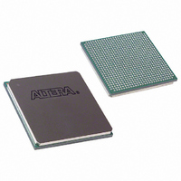
EP1S30F780I6N Altera, EP1S30F780I6N Datasheet - Page 113

EP1S30F780I6N
Manufacturer Part Number
EP1S30F780I6N
Description
IC STRATIX FPGA 30K LE 780-FBGA
Manufacturer
Altera
Series
Stratix®r
Datasheet
1.EP1S10F780C7.pdf
(276 pages)
Specifications of EP1S30F780I6N
Number Of Logic Elements/cells
32470
Number Of Labs/clbs
3247
Total Ram Bits
3317184
Number Of I /o
597
Voltage - Supply
1.425 V ~ 1.575 V
Mounting Type
Surface Mount
Operating Temperature
-40°C ~ 100°C
Package / Case
780-FBGA
Lead Free Status / RoHS Status
Lead free / RoHS Compliant
Number Of Gates
-
Available stocks
Company
Part Number
Manufacturer
Quantity
Price
Company:
Part Number:
EP1S30F780I6N
Manufacturer:
ALTERA
Quantity:
996
- Current page: 113 of 276
- Download datasheet (4Mb)
Altera Corporation
July 2005
The pllenable pin is a dedicated pin that enables/disables PLLs. When
the pllenable pin is low, the clock output ports are driven by GND and
all the PLLs go out of lock. When the pllenable pin goes high again, the
PLLs relock and resynchronize to the input clocks. You can choose which
PLLs are controlled by the pllenable signal by connecting the
pllenable input port of the altpll megafunction to the common
pllenable input pin.
The areset signals are reset/resynchronization inputs for each PLL. The
areset signal should be asserted every time the PLL loses lock to
guarantee correct phase relationship between the PLL output clocks.
Users should include the areset signal in designs if any of the following
conditions are true:
■
■
The device input pins or logic elements (LEs) can drive these input
signals. When driven high, the PLL counters will reset, clearing the PLL
output and placing the PLL out of lock. The VCO will set back to its
nominal setting (~700 MHz). When driven low again, the PLL will
resynchronize to its input as it relocks. If the target VCO frequency is
below this nominal frequency, then the output frequency will start at a
higher value than desired as the PLL locks. If the system cannot tolerate
this, the clkena signal can disable the output clocks until the PLL locks.
The pfdena signals control the phase frequency detector (PFD) output
with a programmable gate. If you disable the PFD, the VCO operates at
its last set value of control voltage and frequency with some long-term
drift to a lower frequency. The system continues running when the PLL
goes out of lock or the input clock is disabled. By maintaining the last
locked frequency, the system has time to store its current settings before
shutting down. You can either use your own control signal or a clkloss
status signal to trigger pfdena.
The clkena signals control the enhanced PLL regional and global
outputs. Each regional and global output port has its own clkena signal.
The clkena signals synchronously disable or enable the clock at the PLL
output port by gating the outputs of the g and l counters. The clkena
signals are registered on the falling edge of the counter output clock to
enable or disable the clock without glitches.
waveform example for a PLL clock port enable. The PLL can remain
locked independent of the clkena signals since the loop-related counters
are not affected. This feature is useful for applications that require a low
power or sleep mode. Upon re-enabling, the PLL does not need a
PLL Reconfiguration or Clock switchover enables in the design.
Phase relationships between output clocks need to be maintained
after a loss of lock condition
Stratix Device Handbook, Volume 1
Figure 2–57
Stratix Architecture
shows the
2–99
Related parts for EP1S30F780I6N
Image
Part Number
Description
Manufacturer
Datasheet
Request
R

Part Number:
Description:
CYCLONE II STARTER KIT EP2C20N
Manufacturer:
Altera
Datasheet:

Part Number:
Description:
CPLD, EP610 Family, ECMOS Process, 300 Gates, 16 Macro Cells, 16 Reg., 16 User I/Os, 5V Supply, 35 Speed Grade, 24DIP
Manufacturer:
Altera Corporation
Datasheet:

Part Number:
Description:
CPLD, EP610 Family, ECMOS Process, 300 Gates, 16 Macro Cells, 16 Reg., 16 User I/Os, 5V Supply, 15 Speed Grade, 24DIP
Manufacturer:
Altera Corporation
Datasheet:

Part Number:
Description:
Manufacturer:
Altera Corporation
Datasheet:

Part Number:
Description:
CPLD, EP610 Family, ECMOS Process, 300 Gates, 16 Macro Cells, 16 Reg., 16 User I/Os, 5V Supply, 30 Speed Grade, 24DIP
Manufacturer:
Altera Corporation
Datasheet:

Part Number:
Description:
High-performance, low-power erasable programmable logic devices with 8 macrocells, 10ns
Manufacturer:
Altera Corporation
Datasheet:

Part Number:
Description:
High-performance, low-power erasable programmable logic devices with 8 macrocells, 7ns
Manufacturer:
Altera Corporation
Datasheet:

Part Number:
Description:
Classic EPLD
Manufacturer:
Altera Corporation
Datasheet:

Part Number:
Description:
High-performance, low-power erasable programmable logic devices with 8 macrocells, 10ns
Manufacturer:
Altera Corporation
Datasheet:

Part Number:
Description:
Manufacturer:
Altera Corporation
Datasheet:

Part Number:
Description:
Manufacturer:
Altera Corporation
Datasheet:

Part Number:
Description:
Manufacturer:
Altera Corporation
Datasheet:

Part Number:
Description:
CPLD, EP610 Family, ECMOS Process, 300 Gates, 16 Macro Cells, 16 Reg., 16 User I/Os, 5V Supply, 25 Speed Grade, 24DIP
Manufacturer:
Altera Corporation
Datasheet:


