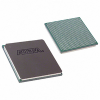
EP1S30F780I6N Altera, EP1S30F780I6N Datasheet - Page 139

EP1S30F780I6N
Manufacturer Part Number
EP1S30F780I6N
Description
IC STRATIX FPGA 30K LE 780-FBGA
Manufacturer
Altera
Series
Stratix®r
Datasheet
1.EP1S10F780C7.pdf
(276 pages)
Specifications of EP1S30F780I6N
Number Of Logic Elements/cells
32470
Number Of Labs/clbs
3247
Total Ram Bits
3317184
Number Of I /o
597
Voltage - Supply
1.425 V ~ 1.575 V
Mounting Type
Surface Mount
Operating Temperature
-40°C ~ 100°C
Package / Case
780-FBGA
Lead Free Status / RoHS Status
Lead free / RoHS Compliant
Number Of Gates
-
Available stocks
Company
Part Number
Manufacturer
Quantity
Price
Company:
Part Number:
EP1S30F780I6N
Manufacturer:
ALTERA
Quantity:
996
- Current page: 139 of 276
- Download datasheet (4Mb)
Figure 2–70. Stratix I/O Banks
Notes to
(1)
(2)
(3)
(4)
(5)
Altera Corporation
July 2005
PLL8
PLL7
PLL1
PLL2
Figure 2–70
will be a reverse view for flip-chip packages.
Figure 2–70
Quartus II software for exact locations.
Banks 9 through 12 are enhanced PLL external clock output banks.
If the high-speed differential I/O pins are not used for high-speed differential signaling, they can support all of the
I/O standards except HSTL Class I and II, GTL, SSTL-18 Class II, PCI, PCI-X 1.0, and AGP 1× /2× .
For guidelines for placing single-ended I/O pads next to differential I/O pads, see the Selectable I/O Standards in
Stratix and Stratix GX Devices chapter in the Stratix Device Handbook, Volume 2.
VREF1B3 VREF2B3 VREF3B3 VREF4B3 VREF5B3
VREF5B8 VREF4B8 VREF3B8 VREF2B8 VREF1B8
DQS9T
DQS9B
Figure
(5)
(5)
2–70:
DQS8T
DQS8B
is a top view of the silicon die. This will correspond to a top-down view for non-flip-chip packages, but
is a graphic representation only. See the device pin-outs on the web (www.altera.com) and the
LVDS, LVPECL, 3.3-V PCML,
and HyperTransport I/O Block
and Regular I/O Pins (4)
LVDS, LVPECL, 3.3-V PCML,
and HyperTransport I/O Block
and Regular I/O Pins (4)
DQS7B
DQS7T
Bank 8
Bank 3
DQS6T
DQS6B
Notes
(1), (2),
DQS5T
DQS5B
I/O Banks 1, 2, 5, and 6 Support All
Single-Ended I/O Standards Except
Differential HSTL Output Clocks,
Differential SSTL-2 Output Clocks,
HSTL Class II, GTL, SSTL-18 Class II,
PCI, PCI-X 1.0, and AGP 1×/2×
I/O Banks 3, 4, 9 & 10 Support
All Single-Ended I/O Standards
I/O Banks 7, 8, 11 & 12 Support
All Single-Ended I/O Standards
(3)
11
9
PLL5
PLL6
10
12
PLL11
PLL12
VREF1B4 VREF2B4 VREF3B4 VREF4B4 VREF5B4
VREF5B7 VREF4B7 VREF3B7 VREF2B7 VREF1B7
DQS4T
DQS4B
and HyperTransport I/O Block
LVDS, LVPECL, 3.3-V PCML,
and HyperTransport I/O Block
LVDS, LVPECL, 3.3-V PCML,
Stratix Device Handbook, Volume 1
DQS3B
DQS3T
and Regular I/O Pins (4)
and Regular I/O Pins (4)
DQS2T
DQS2B
Bank 7
Bank 4
DQS1T
DQS1B
Stratix Architecture
(5)
(5)
DQS0B
DQS0T
PLL10
PLL4
PLL3
PLL9
2–125
Related parts for EP1S30F780I6N
Image
Part Number
Description
Manufacturer
Datasheet
Request
R

Part Number:
Description:
CYCLONE II STARTER KIT EP2C20N
Manufacturer:
Altera
Datasheet:

Part Number:
Description:
CPLD, EP610 Family, ECMOS Process, 300 Gates, 16 Macro Cells, 16 Reg., 16 User I/Os, 5V Supply, 35 Speed Grade, 24DIP
Manufacturer:
Altera Corporation
Datasheet:

Part Number:
Description:
CPLD, EP610 Family, ECMOS Process, 300 Gates, 16 Macro Cells, 16 Reg., 16 User I/Os, 5V Supply, 15 Speed Grade, 24DIP
Manufacturer:
Altera Corporation
Datasheet:

Part Number:
Description:
Manufacturer:
Altera Corporation
Datasheet:

Part Number:
Description:
CPLD, EP610 Family, ECMOS Process, 300 Gates, 16 Macro Cells, 16 Reg., 16 User I/Os, 5V Supply, 30 Speed Grade, 24DIP
Manufacturer:
Altera Corporation
Datasheet:

Part Number:
Description:
High-performance, low-power erasable programmable logic devices with 8 macrocells, 10ns
Manufacturer:
Altera Corporation
Datasheet:

Part Number:
Description:
High-performance, low-power erasable programmable logic devices with 8 macrocells, 7ns
Manufacturer:
Altera Corporation
Datasheet:

Part Number:
Description:
Classic EPLD
Manufacturer:
Altera Corporation
Datasheet:

Part Number:
Description:
High-performance, low-power erasable programmable logic devices with 8 macrocells, 10ns
Manufacturer:
Altera Corporation
Datasheet:

Part Number:
Description:
Manufacturer:
Altera Corporation
Datasheet:

Part Number:
Description:
Manufacturer:
Altera Corporation
Datasheet:

Part Number:
Description:
Manufacturer:
Altera Corporation
Datasheet:

Part Number:
Description:
CPLD, EP610 Family, ECMOS Process, 300 Gates, 16 Macro Cells, 16 Reg., 16 User I/Os, 5V Supply, 25 Speed Grade, 24DIP
Manufacturer:
Altera Corporation
Datasheet:


