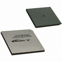
EP2S90F1508I4 Altera, EP2S90F1508I4 Datasheet - Page 134

EP2S90F1508I4
Manufacturer Part Number
EP2S90F1508I4
Description
IC STRATIX II FPGA 90K 1508-FBGA
Manufacturer
Altera
Series
Stratix® IIr
Datasheet
1.EP2S15F484I4N.pdf
(238 pages)
Specifications of EP2S90F1508I4
Number Of Logic Elements/cells
90960
Number Of Labs/clbs
4548
Total Ram Bits
4520488
Number Of I /o
902
Voltage - Supply
1.15 V ~ 1.25 V
Mounting Type
Surface Mount
Operating Temperature
-40°C ~ 100°C
Package / Case
1508-FBGA
Lead Free Status / RoHS Status
Contains lead / RoHS non-compliant
Number Of Gates
-
Other names
544-1923
EP2S90F1508I4
EP2S90F1508I4
Available stocks
Company
Part Number
Manufacturer
Quantity
Price
Company:
Part Number:
EP2S90F1508I4
Manufacturer:
ALTERA
Quantity:
3 000
Company:
Part Number:
EP2S90F1508I4N
Manufacturer:
ALTERA
Quantity:
586
- Current page: 134 of 238
- Download datasheet (3Mb)
Hot Socketing Feature Implementation in Stratix II Devices
4–4
Stratix II Device Handbook, Volume 1
Figure 4–1. Hot Socketing Circuit Block Diagram for Stratix II Devices
The POR circuit monitors V
stated until the device is in user mode. The weak pull-up resistor (R) from
the I/O pin to V
3.3-V tolerance control circuit permits the I/O pins to be driven by 3.3 V
before V
the I/O pins from driving out when the device is not in user mode. The
hot socket circuit prevents I/O pins from internally powering V
V
powered.
Figure 4–2
I/O buffers. This design ensures that the output buffers do not drive
when V
than V
insertion. There is no current path from signal I/O pins to V
or V
tolerant circuit capacitance.
CCINT
Resistor
Pull-Up
CCPD
Weak
PAD
, and V
CCIO
CCIO
CCIO
during hot insertion. The V
. This also applies for sudden voltage spikes during hot
shows a transistor level cross section of the Stratix II device
is powered before V
and/or V
CCPD
R
CCIO
when driven by external signals before the device is
Output
is present to keep the I/O pins from floating. The
CCINT
CCINT
and/or V
CCINT
voltage level and keeps I/O pins tri-
PAD
Input Buffer
to Logic Array
CCPD
Tolerance
or if the I/O pad voltage is higher
Voltage
Control
leakage current charges the 3.3-V
are powered, and it prevents
Output Enable
Altera Corporation
Hot Socket
Pre-Driver
Output
CCINT
Power On
Monitor
Reset
May 2007
CCIO
or V
,
CCIO
Related parts for EP2S90F1508I4
Image
Part Number
Description
Manufacturer
Datasheet
Request
R

Part Number:
Description:
CYCLONE II STARTER KIT EP2C20N
Manufacturer:
Altera
Datasheet:

Part Number:
Description:
CPLD, EP610 Family, ECMOS Process, 300 Gates, 16 Macro Cells, 16 Reg., 16 User I/Os, 5V Supply, 35 Speed Grade, 24DIP
Manufacturer:
Altera Corporation
Datasheet:

Part Number:
Description:
CPLD, EP610 Family, ECMOS Process, 300 Gates, 16 Macro Cells, 16 Reg., 16 User I/Os, 5V Supply, 15 Speed Grade, 24DIP
Manufacturer:
Altera Corporation
Datasheet:

Part Number:
Description:
Manufacturer:
Altera Corporation
Datasheet:

Part Number:
Description:
CPLD, EP610 Family, ECMOS Process, 300 Gates, 16 Macro Cells, 16 Reg., 16 User I/Os, 5V Supply, 30 Speed Grade, 24DIP
Manufacturer:
Altera Corporation
Datasheet:

Part Number:
Description:
High-performance, low-power erasable programmable logic devices with 8 macrocells, 10ns
Manufacturer:
Altera Corporation
Datasheet:

Part Number:
Description:
High-performance, low-power erasable programmable logic devices with 8 macrocells, 7ns
Manufacturer:
Altera Corporation
Datasheet:

Part Number:
Description:
Classic EPLD
Manufacturer:
Altera Corporation
Datasheet:

Part Number:
Description:
High-performance, low-power erasable programmable logic devices with 8 macrocells, 10ns
Manufacturer:
Altera Corporation
Datasheet:

Part Number:
Description:
Manufacturer:
Altera Corporation
Datasheet:

Part Number:
Description:
Manufacturer:
Altera Corporation
Datasheet:

Part Number:
Description:
Manufacturer:
Altera Corporation
Datasheet:

Part Number:
Description:
CPLD, EP610 Family, ECMOS Process, 300 Gates, 16 Macro Cells, 16 Reg., 16 User I/Os, 5V Supply, 25 Speed Grade, 24DIP
Manufacturer:
Altera Corporation
Datasheet:


