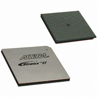
EP2S90F1508I4 Altera, EP2S90F1508I4 Datasheet - Page 140

EP2S90F1508I4
Manufacturer Part Number
EP2S90F1508I4
Description
IC STRATIX II FPGA 90K 1508-FBGA
Manufacturer
Altera
Series
Stratix® IIr
Datasheet
1.EP2S15F484I4N.pdf
(238 pages)
Specifications of EP2S90F1508I4
Number Of Logic Elements/cells
90960
Number Of Labs/clbs
4548
Total Ram Bits
4520488
Number Of I /o
902
Voltage - Supply
1.15 V ~ 1.25 V
Mounting Type
Surface Mount
Operating Temperature
-40°C ~ 100°C
Package / Case
1508-FBGA
Lead Free Status / RoHS Status
Contains lead / RoHS non-compliant
Number Of Gates
-
Other names
544-1923
EP2S90F1508I4
EP2S90F1508I4
Available stocks
Company
Part Number
Manufacturer
Quantity
Price
Company:
Part Number:
EP2S90F1508I4
Manufacturer:
ALTERA
Quantity:
3 000
Company:
Part Number:
EP2S90F1508I4N
Manufacturer:
ALTERA
Quantity:
586
Operating Conditions
5–4
Stratix II Device Handbook, Volume 1
Notes to
(1)
(2)
(3)
(4)
I
R
V
V
V
V
Symbol
CCI00
Table 5–4. Stratix II Device DC Operating Conditions (Part 2 of 2)
Table 5–5. LVTTL Specifications (Part 1 of 2)
CCIO
I H
IL
OH
CONF
Symbol
Typical values are for T
This value is specified for normal device operation. The value may vary during power-up. This applies for all
V
Maximum values depend on the actual T
Estimator (available at www.altera.com) or the Quartus II PowerPlay Power Analyzer feature for maximum
values. See the section
Pin pull-up resistance values are lower if an external source drives the pin higher than V
(1)
CCIO
(4)
Table
settings (3.3, 2.5, 1.8, and 1.5 V).
V
(standby)
Value of I/O pin pull-up
resistor before and
during configuration
Recommended value of
I/O pin external
pull-down resistor before
and during configuration
CCIO
Output supply voltage
High-level input voltage
Low-level input voltage
High-level output voltage
5–4:
supply current
Parameter
Parameter
“Power Consumption” on page 5–20
A
= 25°C, V
I/O Standard Specifications
Tables 5–5
specifications.
V
load, no toggling
inputs
T
Vi = 0; V
Vi = 0; V
Vi = 0; V
Vi = 0; V
Vi = 0; V
CCINT
J
I
= ground, no
= 25° C
through
= 1.2 V, and V
J
and design utilization. See the Excel-based PowerPlay Early Power
CCIO
CCIO
CCIO
CCIO
CCIO
I
OH
Conditions
= 3.3 V
= 2.5 V
= 1.8 V
= 1.5 V
= 1.2 V
= –4 mA
5–32
Conditions
CCIO
show the Stratix II device family I/O standard
EP2S15
EP2S30
EP2S60
EP2S90
EP2S130
EP2S180
(2)
= 1.5 V, 1.8 V, 2.5 V, and 3.3 V.
for more information.
Minimum Typical Maximum Unit
Note (1)
10
15
30
40
50
Minimum
3.135
–0.3
1.7
2.4
4.0
4.0
4.0
4.0
4.0
4.0
25
35
50
75
90
1
CCIO
Altera Corporation
.
Maximum
3.465
4.0
0.8
100
150
170
(3)
(3)
(3)
(3)
(3)
(3)
50
70
2
April 2011
mA
mA
mA
mA
mA
mA
Unit
kΩ
kΩ
kΩ
kΩ
kΩ
kΩ
V
V
V
V


