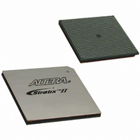
EP2S90F1508I4 Altera, EP2S90F1508I4 Datasheet - Page 145

EP2S90F1508I4
Manufacturer Part Number
EP2S90F1508I4
Description
IC STRATIX II FPGA 90K 1508-FBGA
Manufacturer
Altera
Series
Stratix® IIr
Datasheet
1.EP2S15F484I4N.pdf
(238 pages)
Specifications of EP2S90F1508I4
Number Of Logic Elements/cells
90960
Number Of Labs/clbs
4548
Total Ram Bits
4520488
Number Of I /o
902
Voltage - Supply
1.15 V ~ 1.25 V
Mounting Type
Surface Mount
Operating Temperature
-40°C ~ 100°C
Package / Case
1508-FBGA
Lead Free Status / RoHS Status
Contains lead / RoHS non-compliant
Number Of Gates
-
Other names
544-1923
EP2S90F1508I4
EP2S90F1508I4
Available stocks
Company
Part Number
Manufacturer
Quantity
Price
Company:
Part Number:
EP2S90F1508I4
Manufacturer:
ALTERA
Quantity:
3 000
Company:
Part Number:
EP2S90F1508I4N
Manufacturer:
ALTERA
Quantity:
586
- Current page: 145 of 238
- Download datasheet (3Mb)
Altera Corporation
April 2011
Note to
(1)
V
V
V
V
V
R
V
V
V
V
Δ V
V
Δ V
R
V
V
Table 5–12. LVPECL Specifications
Table 5–13. HyperTransport Technology Specifications
Table 5–14. 3.3-V PCI Specifications (Part 1 of 2)
Symbol
Symbol
Symbol
CCIO
ID
ICM
OD
OCM
CCIO
ID
ICM
OD
OCM
CCIO
IH
L
L
OD
OCM
The top and bottom clock input differential buffers in I/O banks 3, 4, 7, and 8 are powered by V
The PLL clock output/feedback differential buffers are powered by VCC_PLL_OUT. For differential clock
output/feedback operation, VCC_PLL_OUT should be connected to 3.3 V.
(1)
Table
I/O supply voltage
Input differential voltage
swing (single-ended)
Input common mode voltage
Output differential voltage
(single-ended)
Output common mode
voltage
Receiver differential input
resistor
I/O supply voltage for left and
right I/O banks (1, 2, 5, and 6)
Input differential voltage swing
(single-ended)
Input common mode voltage
Output differential voltage
(single-ended)
Change in V
and low
Output common mode voltage R
Change in V
and low
Receiver differential input
resistor
Output supply voltage
High-level input voltage
5–12:
Parameter
Parameter
Parameter
OCM
OD
between high
between high
R
R
L
L
R
R
R
R
R
= 100 Ω
= 100 Ω
Conditions
L
L
L
L
L
L
Conditions
Conditions
= 100 Ω
= 100 Ω
= 100 Ω
= 100 Ω
= 100 Ω
= 100 Ω
0.5 × V
Minimum
Minimum
Minimum
3.135
1,650
2.375
300
525
300
385
400
440
1.0
3.0
90
90
CCIO
Stratix II Device Handbook, Volume 1
DC & Switching Characteristics
Typical
Typical
Typical
3.300
2.500
600
100
600
600
600
600
100
3.3
V
Maximum
Maximum
Maximum
CCIO
CCINT
3.465
1,000
2,250
2.625
970
110
900
845
820
780
110
2.5
3.6
75
50
+ 0.5
, not V
CCIO
Unit
Unit
Unit
mV
mV
mV
mV
mV
mV
mV
mV
mV
5–9
V
V
Ω
Ω
V
V
V
.
Related parts for EP2S90F1508I4
Image
Part Number
Description
Manufacturer
Datasheet
Request
R

Part Number:
Description:
CYCLONE II STARTER KIT EP2C20N
Manufacturer:
Altera
Datasheet:

Part Number:
Description:
CPLD, EP610 Family, ECMOS Process, 300 Gates, 16 Macro Cells, 16 Reg., 16 User I/Os, 5V Supply, 35 Speed Grade, 24DIP
Manufacturer:
Altera Corporation
Datasheet:

Part Number:
Description:
CPLD, EP610 Family, ECMOS Process, 300 Gates, 16 Macro Cells, 16 Reg., 16 User I/Os, 5V Supply, 15 Speed Grade, 24DIP
Manufacturer:
Altera Corporation
Datasheet:

Part Number:
Description:
Manufacturer:
Altera Corporation
Datasheet:

Part Number:
Description:
CPLD, EP610 Family, ECMOS Process, 300 Gates, 16 Macro Cells, 16 Reg., 16 User I/Os, 5V Supply, 30 Speed Grade, 24DIP
Manufacturer:
Altera Corporation
Datasheet:

Part Number:
Description:
High-performance, low-power erasable programmable logic devices with 8 macrocells, 10ns
Manufacturer:
Altera Corporation
Datasheet:

Part Number:
Description:
High-performance, low-power erasable programmable logic devices with 8 macrocells, 7ns
Manufacturer:
Altera Corporation
Datasheet:

Part Number:
Description:
Classic EPLD
Manufacturer:
Altera Corporation
Datasheet:

Part Number:
Description:
High-performance, low-power erasable programmable logic devices with 8 macrocells, 10ns
Manufacturer:
Altera Corporation
Datasheet:

Part Number:
Description:
Manufacturer:
Altera Corporation
Datasheet:

Part Number:
Description:
Manufacturer:
Altera Corporation
Datasheet:

Part Number:
Description:
Manufacturer:
Altera Corporation
Datasheet:

Part Number:
Description:
CPLD, EP610 Family, ECMOS Process, 300 Gates, 16 Macro Cells, 16 Reg., 16 User I/Os, 5V Supply, 25 Speed Grade, 24DIP
Manufacturer:
Altera Corporation
Datasheet:


