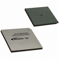
EP2S90F1508I4 Altera, EP2S90F1508I4 Datasheet - Page 158

EP2S90F1508I4
Manufacturer Part Number
EP2S90F1508I4
Description
IC STRATIX II FPGA 90K 1508-FBGA
Manufacturer
Altera
Series
Stratix® IIr
Datasheet
1.EP2S15F484I4N.pdf
(238 pages)
Specifications of EP2S90F1508I4
Number Of Logic Elements/cells
90960
Number Of Labs/clbs
4548
Total Ram Bits
4520488
Number Of I /o
902
Voltage - Supply
1.15 V ~ 1.25 V
Mounting Type
Surface Mount
Operating Temperature
-40°C ~ 100°C
Package / Case
1508-FBGA
Lead Free Status / RoHS Status
Contains lead / RoHS non-compliant
Number Of Gates
-
Other names
544-1923
EP2S90F1508I4
EP2S90F1508I4
Available stocks
Company
Part Number
Manufacturer
Quantity
Price
Company:
Part Number:
EP2S90F1508I4
Manufacturer:
ALTERA
Quantity:
3 000
Company:
Part Number:
EP2S90F1508I4N
Manufacturer:
ALTERA
Quantity:
586
Timing Model
5–22
Stratix II Device Handbook, Volume 1
Figure 5–3. Input Register Setup & Hold Timing Diagram
For output timing, different I/O standards require different baseline
loading techniques for reporting timing delays. Altera characterizes
timing delays with the required termination for each I/O standard and
with 0 pF (except for PCI and PCI-X which use 10 pF) loading and the
timing is specified up to the output pin of the FPGA device. The
Quartus II software calculates the I/O timing for each I/O standard with
a default baseline loading as specified by the I/O standards.
The following measurements are made during device characterization.
Altera measures clock-to-output delays (t
minimum voltage, and maximum temperature (PVT) for default loading
conditions shown in
clock pin to output pin timing for Stratix II devices.
Simulation using IBIS models is required to determine the delays on the
PCB traces in addition to the output pin delay timing reported by the
Quartus II software and the timing model in the device handbook.
1.
2.
3.
t
register + IOE output register clock-to-output delay + delay from
output register to output pin + I/O output delay
t
output register + IOE output register clock-to-output delay + delay
from output register to output pin + I/O output delay + output
enable pin delay
Simulate the output driver of choice into the generalized test setup,
using values from
Record the time to V
Simulate the output driver of choice into the actual PCB trace and
load, using the appropriate IBIS model or capacitance value to
represent the load.
CO
xz
/t
from clock pin to I/O pin = delay from clock pad to I/O output
zx
from clock pin to I/O pin = delay from clock pad to I/O
Table
Input Clock Delay
Input Data Delay
Table
MEAS
5–34. Use the following equations to calculate
5–34.
.
CO
) at worst-case process,
micro t
micro t
SU
H
Altera Corporation
April 2011


