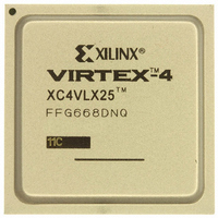
XC4VLX25-11FFG668C Xilinx Inc, XC4VLX25-11FFG668C Datasheet - Page 10

XC4VLX25-11FFG668C
Manufacturer Part Number
XC4VLX25-11FFG668C
Description
IC FPGA VIRTEX-4 24K 668-FCBGA
Manufacturer
Xilinx Inc
Series
Virtex™-4r
Specifications of XC4VLX25-11FFG668C
Number Of Logic Elements/cells
24192
Number Of Labs/clbs
2688
Total Ram Bits
1327104
Number Of I /o
448
Voltage - Supply
1.14 V ~ 1.26 V
Mounting Type
Surface Mount
Operating Temperature
0°C ~ 85°C
Package / Case
668-BBGA, FCBGA
Package
668FCBGA
Family Name
Virtex®-4
Device Logic Units
24192
Typical Operating Supply Voltage
1.2 V
Maximum Number Of User I/os
448
Ram Bits
1327104
For Use With
807-1004 - DAUGHTER CARD WITH VIRTEX-4HW-AFX-FF668-400 - BOARD DEV VIRTEX 4 FF668122-1523 - EVALUATION PLATFORM VIRTEX-4
Lead Free Status / RoHS Status
Lead free / RoHS Compliant
Number Of Gates
-
Other names
122-1490
Available stocks
Company
Part Number
Manufacturer
Quantity
Price
Company:
Part Number:
XC4VLX25-11FFG668C
Manufacturer:
XILINX
Quantity:
101
Company:
Part Number:
XC4VLX25-11FFG668C
Manufacturer:
Xilinx Inc
Quantity:
10 000
Part Number:
XC4VLX25-11FFG668C
Manufacturer:
XILINX/赛灵思
Quantity:
20 000
Extended LVDS DC Specifications (LVDSEXT_25)
Table 10: Extended LVDS DC Specifications
LVPECL DC Specifications (LVPECL_25)
These values are valid when driving a 100Ω differential load
only, i.e., a 100Ω resistor between the two receiver pins.
The V
and are compatible with devices tolerant of lower com-
Table 11: LVPECL DC Specifications
DS302 (v3.7) September 9, 2009
Product Specification
Notes:
1.
2.
Notes:
1.
2.
V
V
V
V
Symbol
V
OH
OL
ICM
IDIFF
V
V
V
Symbol
V
V
V
ODIFF
IDIFF
OCM
CCO
Recommended input maximum voltage not to exceed V
Recommended input minimum voltage not to go below –0.5V.
Recommended input maximum voltage not to exceed V
Recommended input minimum voltage not to go below –0.5V.
ICM
OH
OL
OH
levels are 200 mV below standard LVPECL levels
Supply Voltage
Output High Voltage for Q and Q
Output Low Voltage for Q and Q
Differential Output Voltage (Q – Q),
Q = High (Q – Q), Q = High
Output Common-Mode Voltage
Differential Input Voltage
(Q – Q), Q = High (Q – Q), Q = High
Input Common-Mode Voltage
Output High Voltage
Output Low Voltage
Input Common-Mode Voltage
Differential Input Voltage
DC Parameter
DC Parameter
(1,2)
(1,2)
CC0
CC0
R
R
R
R
Common-mode input voltage = 1.25V
Differential input voltage = ±350 mV
T
T
T
T
+ 0.2V.
+ 0.2V.
= 100Ω across Q and Q signals
= 100Ω across Q and Q signals
= 100Ω across Q and Q signals
= 100Ω across Q and Q signals
www.xilinx.com
Virtex-4 FPGA Data Sheet: DC and Switching Characteristics
Conditions
V
mon-mode ranges.
specifications of LVPECL. For more information on using
LVPECL
SelectIO Resources.
V
CC
CC
0.100
Min
0.6
– 1.025
– 1.81
,
see the
Virtex-4 FPGA User
Table 11
1.545
0.795
Typ
0.715
1.125
2.38
Min
440
100
0.3
–
summarizes the DC output
1.250
Typ
2.5
1.2
V
V
–
–
–
–
CC
CC
Max
2.2
1.5
Guide: Chapter 6,
– 0.88
– 1.62
1.785
1.375
1000
2.63
Max
820
2.2
–
Units
Units
mV
mV
V
V
V
V
V
V
V
V
V
10


