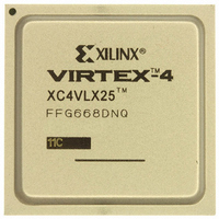
XC4VLX25-11FFG668C Xilinx Inc, XC4VLX25-11FFG668C Datasheet - Page 13

XC4VLX25-11FFG668C
Manufacturer Part Number
XC4VLX25-11FFG668C
Description
IC FPGA VIRTEX-4 24K 668-FCBGA
Manufacturer
Xilinx Inc
Series
Virtex™-4r
Specifications of XC4VLX25-11FFG668C
Number Of Logic Elements/cells
24192
Number Of Labs/clbs
2688
Total Ram Bits
1327104
Number Of I /o
448
Voltage - Supply
1.14 V ~ 1.26 V
Mounting Type
Surface Mount
Operating Temperature
0°C ~ 85°C
Package / Case
668-BBGA, FCBGA
Package
668FCBGA
Family Name
Virtex®-4
Device Logic Units
24192
Typical Operating Supply Voltage
1.2 V
Maximum Number Of User I/os
448
Ram Bits
1327104
For Use With
807-1004 - DAUGHTER CARD WITH VIRTEX-4HW-AFX-FF668-400 - BOARD DEV VIRTEX 4 FF668122-1523 - EVALUATION PLATFORM VIRTEX-4
Lead Free Status / RoHS Status
Lead free / RoHS Compliant
Number Of Gates
-
Other names
122-1490
Available stocks
Company
Part Number
Manufacturer
Quantity
Price
Company:
Part Number:
XC4VLX25-11FFG668C
Manufacturer:
XILINX
Quantity:
101
Company:
Part Number:
XC4VLX25-11FFG668C
Manufacturer:
Xilinx Inc
Quantity:
10 000
Part Number:
XC4VLX25-11FFG668C
Manufacturer:
XILINX/赛灵思
Quantity:
20 000
Since individual family members are produced at different
times, the migration from one category to another depends
completely on the status of the fabrication process for each
device.
Testing of Switching Characteristics
All devices are 100% functionally tested. Internal timing
parameters are derived from measuring internal test pat-
terns. Listed below are representative values. For more
specific, more precise, and worst-case guaranteed data,
PowerPC Switching Characteristics
Consult the
Table 15: PowerPC 405 Processor Clocks Absolute AC Characteristics
DS302 (v3.7) September 9, 2009
Product Specification
Notes:
1.
2.
3.
4.
Characteristics when APU Not Used
Characteristics when APU Used
CPMC405CLOCK frequency
CPMDCRCLK
CPMFCMCLK
JTAGC405TCK frequency
PLBCLK
BRAMDSOCMCLK
BRAMISOCMCLK
CPMC405CLOCK frequency
CPMDCRCLK
CPMFCMCLK
JTAGC405TCK frequency
PLBCLK
BRAMDSOCMCLK
BRAMISOCMCLK
Worst-case DCM output clock jitter is included in these specifications.
The theoretical maximum frequency of this clock is one-half the CPMC405CLOCK. However, the achievable maximum is system dependent, and will
be much less.
The theoretical maximum frequency of these clocks is equal to the CPMC405CLOCK. Integer clock ratios are required for the CPMC405CLOCK and
BRAMDSOCMCLK, CPMC405CLOCK and BRAMISOCMCLK, CPMC405CLOCK and CPMDCRCLK, CPMC405CLOCK and CPMFCMCLK, and
CPMC405CLOCK and PLBCLK. The integer ratios can be different for each interface. However, the achievable maximum is system dependent.
Maximum operating frequency of CPMC405CLOCK is specified with the input pin TIEC405DISOPERANDFWD connected to a logic 1.
(3)
(3)
PowerPC 405 Processor Block Reference Guide
Description
(3)
(3)
(3)
(3)
(3)
(3)
(3)
(3)
(2)
(2)
(1,4)
(1,4)
Min
NA
0
0
0
0
0
0
0
0
0
0
0
0
0
www.xilinx.com
-12
Virtex-4 FPGA Data Sheet: DC and Switching Characteristics
166.5
Max
450
450
225
450
450
450
333
333
333
333
333
333
NA
for further information.
All specifications are always representative of worst-case
supply voltage and junction temperature conditions.
use the values reported by the static timing analyzer (TRCE
in the Xilinx Development System) and back-annotate to the
simulation net list. Unless otherwise noted, values apply to
all Virtex-4 devices.
Min
Speed Grade
NA
0
0
0
0
0
0
0
0
0
0
0
0
0
-11
137.5
Max
400
400
200
400
400
400
275
275
275
275
275
275
NA
Min
NA
0
0
0
0
0
0
0
0
0
0
0
0
0
-10
116.5
Max
350
350
175
350
350
350
233
233
233
233
233
233
NA
Units
MHz
MHz
MHz
MHz
MHz
MHz
MHz
MHz
MHz
MHz
MHz
MHz
MHz
MHz
13


