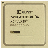
XC4VLX25-11FFG668C Xilinx Inc, XC4VLX25-11FFG668C Datasheet - Page 42

XC4VLX25-11FFG668C
Manufacturer Part Number
XC4VLX25-11FFG668C
Description
IC FPGA VIRTEX-4 24K 668-FCBGA
Manufacturer
Xilinx Inc
Series
Virtex™-4r
Specifications of XC4VLX25-11FFG668C
Number Of Logic Elements/cells
24192
Number Of Labs/clbs
2688
Total Ram Bits
1327104
Number Of I /o
448
Voltage - Supply
1.14 V ~ 1.26 V
Mounting Type
Surface Mount
Operating Temperature
0°C ~ 85°C
Package / Case
668-BBGA, FCBGA
Package
668FCBGA
Family Name
Virtex®-4
Device Logic Units
24192
Typical Operating Supply Voltage
1.2 V
Maximum Number Of User I/os
448
Ram Bits
1327104
For Use With
807-1004 - DAUGHTER CARD WITH VIRTEX-4HW-AFX-FF668-400 - BOARD DEV VIRTEX 4 FF668122-1523 - EVALUATION PLATFORM VIRTEX-4
Lead Free Status / RoHS Status
Lead free / RoHS Compliant
Number Of Gates
-
Other names
122-1490
Available stocks
Company
Part Number
Manufacturer
Quantity
Price
Company:
Part Number:
XC4VLX25-11FFG668C
Manufacturer:
XILINX
Quantity:
101
Company:
Part Number:
XC4VLX25-11FFG668C
Manufacturer:
Xilinx Inc
Quantity:
10 000
Part Number:
XC4VLX25-11FFG668C
Manufacturer:
XILINX/赛灵思
Quantity:
20 000
Table 50: Miscellaneous Timing Parameters
DS302 (v3.7) September 9, 2009
Product Specification
Notes:
1.
2.
3.
4.
5.
6.
7.
Time Required to Achieve LOCK
Fine Phase Shifting
Delay Lines
Input Signal Requirements
T_LOCK_DLL_240
T_LOCK_DLL_120_240
T_LOCK_DLL_60_120
T_LOCK_DLL_50_60
T_LOCK_DLL_40_50
T_LOCK_DLL_30_40
T_LOCK_DLL_24_30
T_LOCK_DLL_30
T_LOCK_FX_MAX
T_LOCK_DLL_FINE_SHIFT
FINE_SHIFT_RANGE_MS
FINE_SHIFT_RANGE_MR
DCM_TAP_MS_MIN
DCM_TAP_MS_MAX
DCM_TAP_MR_MIN
DCM_TAP_MR_MAX
DCM_RESET
DCM_INPUT_CLOCK_STOP
For boundary frequencies, choose the higher delay.
DLL Outputs are used in these instances to describe the outputs: CLK0, CLK90, CLK180, CLK270, CLK2X, CLK2X180, and CLKDV.
DFS Outputs are used in these instances to describe the outputs: CLKFX and CLKFX180.
CLKIN must be present and stable during the DCM_RESET.
This only applies to production step 1 LX and SX devices. For these devices, use the design solutions described in Answer Record 21127 for support
of longer reset durations. Production step 2 LX and SX devices and all production FX devices do not have this requirement.
For production step 1 LX and SX devices, use the design solutions described in Answer Record 21127 for support of longer durations of stopped
clocks. For production step 2 LX and SX devices and all production FX devices, the ISE software automatically inserts a small macro to support
longer durations of stopped clocks.
For all stepping levels, once the input clock is toggling again and stable after being stopped, DCM must be reset.
Symbol
(4)
DLL output – Frequency range > 240 MHz
DLL output – Frequency range 120 - 240 MHz
DLL output – Frequency range 60 - 120 MHz
DLL output – Frequency range 50 - 60 MHz
DLL output – Frequency range 40 - 50 MHz
DLL output – Frequency range 30 - 40 MHz
DLL output – Frequency range 24 - 30 MHz
DLL output – Frequency range < 30 MHz
DFS outputs
Multiplication factor for DLL lock time with Fine Shift
Absolute shifting range in maximum speed mode
Absolute shifting range in maximum range mode
Tap delay resolution (Min) in maximum speed mode
Tap delay resolution (Max) in maximum speed mode
Tap delay resolution (Min) in maximum range mode
Tap delay resolution (Max) in maximum range mode
Minimum duration that RST must be held asserted
Maximum duration that RST can be held asserted
Maximum duration that CLKIN and CLKFB can be
stopped
(6,7)
(3)
www.xilinx.com
Description
Virtex-4 FPGA Data Sheet: DC and Switching Characteristics
(2)
(2)
(1,2)
(1,2)
(1,2)
(1,2)
(1,2)
(1,2)
(5)
1250
1250
200
100
-12
225
325
500
900
40
10
20
63
10
10
10
60
2
7
5
Speed Grade
1250
1250
200
100
-11
225
325
500
900
10
20
63
10
10
40
10
60
2
7
5
1250
1250
200
100
225
325
500
900
-10
20
63
10
10
40
10
60
10
2
7
5
Units
sec
ms
ms
ms
µs
µs
µs
µs
µs
µs
µs
µs
ns
ns
ps
ps
ps
ps
42


