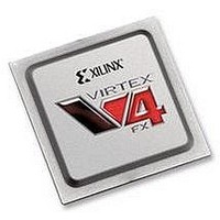
XC4VFX60-10FFG1152C Xilinx Inc, XC4VFX60-10FFG1152C Datasheet - Page 3

XC4VFX60-10FFG1152C
Manufacturer Part Number
XC4VFX60-10FFG1152C
Description
IC FPGA VIRTEX-4 FX 60K 1152FBGA
Manufacturer
Xilinx Inc
Series
Virtex™-4r
Datasheets
1.XC4VFX12-10FFG668C.pdf
(58 pages)
2.XC4VFX12-10FFG668C.pdf
(9 pages)
3.XC4VFX12-10FFG668C.pdf
(406 pages)
Specifications of XC4VFX60-10FFG1152C
Total Ram Bits
4276224
Number Of Logic Elements/cells
56880
Number Of Labs/clbs
6320
Number Of I /o
576
Voltage - Supply
1.14 V ~ 1.26 V
Mounting Type
Surface Mount
Operating Temperature
0°C ~ 85°C
Package / Case
1152-BBGA, FCBGA
No. Of Logic Blocks
6656
No. Of Macrocells
56880
Family Type
Virtex-4
No. Of Speed Grades
10
No. Of I/o's
576
Clock Management
DCM
Core Supply
RoHS Compliant
Package
1152FCBGA
Family Name
Virtex®-4
Device Logic Units
56880
Typical Operating Supply Voltage
1.2 V
Maximum Number Of User I/os
576
Ram Bits
4276224
Lead Free Status / RoHS Status
Lead free / RoHS Compliant
For Use With
HW-V4-ML410-UNI-G - EVALUATION PLATFORM VIRTEX-4
Number Of Gates
-
Lead Free Status / RoHS Status
Lead free / RoHS Compliant
Available stocks
Company
Part Number
Manufacturer
Quantity
Price
Company:
Part Number:
XC4VFX60-10FFG1152C
Manufacturer:
XilinxInc
Quantity:
3 000
Company:
Part Number:
XC4VFX60-10FFG1152C
Manufacturer:
Xilinx Inc
Quantity:
10 000
Table 2: Recommended Operating Conditions (Continued)
Notes:
1.
2.
3.
4.
5.
6.
7.
Table 3: DC Characteristics Over Recommended Operating Conditions
DS302 (v3.7) September 9, 2009
Product Specification
AVCCAUXRX
AVCCAUXTX
AVCCAUXMGT
I
CCAUXRX
Symbol
Configuration data is retained even if V
V
For 3.3V I/O operation, refer to the
Includes V
The configuration output supply voltage V
IMPORTANT! All unused RocketIO transceivers must be connected to power and GND. When using RocketIO transceivers, refer to the power filtering
section of the
Passive filtering must meet the requirements discussed in the
Internal AC coupling is enabled.
I
V
I
I
Symbol
BATT
RPU
RPD
BATT
V
V
I
DRINT
C
REF
V
TRX
DRI
I
L
IN
TTX
(1)
(1)
(1)
is required only when using bitstream encryption. If battery is not used, connect V
(7)
(2)
CCO
(6)
(6)
Virtex-4 RocketIO Multi-Gigabit Transceiver User
Data retention V
(below which configuration data might be lost)
Data retention V
(below which configuration data might be lost)
V
Input or output leakage current per pin (sample-tested)
Input capacitance (sample-tested)
Pad pull-up (when selected) @ V
Pad pull-up (when selected) @ V
Pad pull-up (when selected) @ V
Pad pull-up (when selected) @ V
Pad pull-up (when selected) @ V
Pad pull-down (when selected) @ V
Battery supply current
Operating AVCCAUXRX supply current
of 1.2V, 1.5V, 1.8V, 2.5V, and 3.3V
REF
Auxiliary receive supply voltage relative to GNDA
Auxiliary transmit supply voltage relative to GNDA
Auxiliary management supply voltage relative to GNDA
Terminal receive supply voltage relative to GND
Terminal transmit supply voltage relative to GND
current per pin
CCINT
CCAUX
Virtex-4 FPGA User
CCO
voltage
voltage
CC_CONFIG
Description
drops to 0V.
Description
IN
IN
IN
IN
IN
is also known as V
= 0V, V
= 0V, V
= 0V, V
= 0V, V
= 0V, V
IN
Guide.
= V
CCO
Virtex-4 RocketIO Multi-Gigabit Transceiver User
www.xilinx.com
Guide. Unused transceivers must be powered by an appropriate voltage level source.
CCO
CCO
CCO
CCO
CCO
Virtex-4 FPGA Data Sheet: DC and Switching Characteristics
= 3.3V
= 3.0V
= 2.5V
= 1.8V
= 1.5V
CCO_0
1.25 Digital RX
BATT
Data Rate
Commercial
Commercial
Commercial
Commercial
Commercial
1.25/2.5
(Gb/s)
Industrial
Industrial
Industrial
Industrial
Industrial
3.125
4.25
to either ground or V
6.5
5.0
Min
0.9
2.0
5
5
5
5
5
5
2.375
2.375
Min
1.14
1.14
1.14
1.14
0.25
0.25
1.14
1.14
Guide.
CCAUX
Typ
292
302
291
279
263
314
75
.
Max
200
125
120
100
100
427
485
446
382
351
432
2.625
2.625
1.575
1.575
10
10
10
60
40
Max
1.26
1.26
1.26
1.26
2.5
2.5
Units
mA
mA
mA
mA
mA
mA
µA
µA
pF
µA
µA
µA
µA
µA
µA
nA
Units
V
V
V
V
V
V
V
V
V
V
V
V
3


