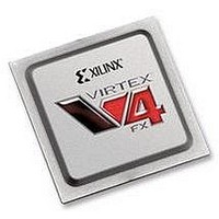
XC4VFX60-10FFG1152C Xilinx Inc, XC4VFX60-10FFG1152C Datasheet - Page 33

XC4VFX60-10FFG1152C
Manufacturer Part Number
XC4VFX60-10FFG1152C
Description
IC FPGA VIRTEX-4 FX 60K 1152FBGA
Manufacturer
Xilinx Inc
Series
Virtex™-4r
Datasheets
1.XC4VFX12-10FFG668C.pdf
(58 pages)
2.XC4VFX12-10FFG668C.pdf
(9 pages)
3.XC4VFX12-10FFG668C.pdf
(406 pages)
Specifications of XC4VFX60-10FFG1152C
Total Ram Bits
4276224
Number Of Logic Elements/cells
56880
Number Of Labs/clbs
6320
Number Of I /o
576
Voltage - Supply
1.14 V ~ 1.26 V
Mounting Type
Surface Mount
Operating Temperature
0°C ~ 85°C
Package / Case
1152-BBGA, FCBGA
No. Of Logic Blocks
6656
No. Of Macrocells
56880
Family Type
Virtex-4
No. Of Speed Grades
10
No. Of I/o's
576
Clock Management
DCM
Core Supply
RoHS Compliant
Package
1152FCBGA
Family Name
Virtex®-4
Device Logic Units
56880
Typical Operating Supply Voltage
1.2 V
Maximum Number Of User I/os
576
Ram Bits
4276224
Lead Free Status / RoHS Status
Lead free / RoHS Compliant
For Use With
HW-V4-ML410-UNI-G - EVALUATION PLATFORM VIRTEX-4
Number Of Gates
-
Lead Free Status / RoHS Status
Lead free / RoHS Compliant
Available stocks
Company
Part Number
Manufacturer
Quantity
Price
Company:
Part Number:
XC4VFX60-10FFG1152C
Manufacturer:
XilinxInc
Quantity:
3 000
Company:
Part Number:
XC4VFX60-10FFG1152C
Manufacturer:
Xilinx Inc
Quantity:
10 000
Block RAM and FIFO Switching Characteristics
Table 40: Block RAM Switching Characteristics
DS302 (v3.7) September 9, 2009
Product Specification
Notes:
1.
2.
3.
4.
5.
Sequential Delays
Setup and Hold Times Before Clock CLK
Maximum Frequency
T
T
T
T
T
T
T
T
F
F
CLK-to-CLK
A Zero “0” Hold Time listing indicates no hold time or a negative hold time. Negative values cannot be guaranteed “best-case,” but if a “0” is listed,
there is no positive hold time.
T
T
T
Xilinx block RAMs do not have asynchronous inputs on an enabled port address. During the time that a port is enabled, its addresses must be stable
during the specified set-up time. Do not create an asynchronous input on an enabled port address.
RCKO_DORA
RCKO_DOA
RCCK_ADDR
RDCK_DI
RCCK_EN
RCCK_REGCE
RCCK_SSR
RCCK_WE
MAX
MAX
RCKO_DORA
RCKO_DOA
RCKO_DI
Symbol
/
includes both A and B inputs as well as the parity inputs of A and B.
/
T
/
T
/
includes T
T
RCKD_DI
T
includes T
/
RCKC_EN
RCKC_WE
RCKC_SSR
T
/
T
RCKC_ADDR
RCKC_REGCE
RCKO_DOPA
RCKO_DOWA
as well as the B port equivalent timing parameters.
Clock CLK to DOUT output (without output register)
Clock CLK to DOUT output with ECC
(without output register)
Clock CLK to DOUT output (with output register)
Clock CLK to DOUT output with ECC (with output
register)
ADDR inputs
DIN inputs
EN input
CE input of output register
RST input
WEN input
Write first and no change mode
Read first mode
Read first mode
, T
RCKO_DOPAR
(5)
(4)
, and T
Description
RCKO_DOPAW
www.xilinx.com
Virtex-4 FPGA Data Sheet: DC and Switching Characteristics
as well as the B port equivalent timing parameters.
(3)
(2)
500.00
500.00
500.00
1.65
3.00
0.72
2.00
0.34
0.26
0.18
0.26
0.41
0.26
0.25
0.26
0.25
0.26
0.59
0.26
-12
Speed Grade
450.45
450.45
450.45
1.83
3.33
0.80
2.20
0.37
0.28
0.20
0.28
0.45
0.28
0.27
0.28
0.27
0.28
0.65
0.28
-11
400.00
400.00
400.00
2.10
3.83
0.92
2.50
0.43
0.33
0.23
0.33
0.52
0.33
0.32
0.33
0.32
0.33
0.75
0.33
-10
ns, Max
ns, Max
ns, Max
ns, Max
ns, Min
ns, Min
ns, Min
ns, Min
ns, Min
ns, Min
Units
MHz
MHz
MHz
33


