PNX1502E/G,557 NXP Semiconductors, PNX1502E/G,557 Datasheet - Page 339
PNX1502E/G,557
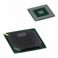
Manufacturer Part Number
PNX1502E/G,557
Description
IC MEDIA PROC 300MHZ 456-BGA
Manufacturer
NXP Semiconductors
Specifications of PNX1502E/G,557
Applications
Multimedia
Core Processor
TriMedia
Controller Series
Nexperia
Interface
I²C, 2-Wire Serial
Number Of I /o
61
Voltage - Supply
1.23 V ~ 1.37 V
Operating Temperature
0°C ~ 85°C
Mounting Type
Surface Mount
Package / Case
456-BGA
Lead Free Status / RoHS Status
Lead free / RoHS Compliant
Program Memory Type
-
Ram Size
-
Lead Free Status / Rohs Status
Compliant
Other names
568-1298
935277748557
PNX1502E/G
935277748557
PNX1502E/G


Philips Semiconductors
Volume 1 of 1
Table 9: Register Description
PNX15XX_SER_3
Product data sheet
Bit
2
1
0
Offset 0x06 5004
Note: Addressing modes 2048_MODE, 1024_MODE, and the interleaving mode defined by the BANK_SWITCH field are
mutually exclusive. Setting 2048_MODE to ‘1’ sets the IP_2031 into 2048 byte stride mode, and makes the values of
1024_MODE and BANK_SWITCH “don’t cares” for the IP_2031. When 2048_MODE is ‘0’ and 1024_MODE is ‘1’, the
IP_2031 is set into 1024 byte stride mode, which makes the value of BANK_SWITCH a “don’t care” for the IP_2031.
31:4
3:0
Offset 0x06 5008
31
30:0
The address locations of the DDR memory ranks are determined by registers RANK0_ADDR_LO, RANK0_ADDR_HI, and
RANK1_ADDR_HI. Addresses in [RANK0_ADDR_LO, RANK0_ADDR_HI] are directed to rank 0, addresses in
[RANK0_ADDR_HI, RANK1_ADDR_HI] are directed to rank 1. Addresses outside the two ranks are said to cause an
address error.
Offset 0x06 5010
31:0
Offset 0x06 5014
31:0
Offset 0x06 5018
31:0
Dimension of DDR Memories
Offset 0x06 5080
31:13
Symbol
DDR_HALVE_WIDTH
SPEC_AUTO_PR
START
Unused
BANK_SWITCH
PON
LIMIT
ADDR_LO
ADDR_HI
ADDR_HI
Unused
DDR_DEF_BANK_SWITCH
AUTO_HALT_LIMIT
RANK0_ADDR_LO
RANK0_ADDR_HI
RANK1_ADDR_HI
DDR_MR
Access Value
R/W
R/W
R/W
R
R/W
R/W
R/W
R/W
R/W
R/W
R
0
0
0
-
3
0
-
0x0000
0000
0xFFFF
FFFF
0xFFFF
FFFF
-
Rev. 3 — 17 March 2006
Description
‘0’: The complete “dq” bus of the DDR interface is used.
‘1’: Only the lower halve of the data bus of the DDR interface is
used. Only DDR data bits “MM_DATA[15:0]” are in use.
‘0’: Speculative auto precharge is off.
‘1’: Speculative auto precharge is on.
‘1’: Start DDR controller. When started, controller will return the
start bit to ‘0’.
These bits should be ignored when read and written as 0s.
Switch banks every 2^BANK_SWITCH columns (each column has
a width of 4 bytes). For 32-byte interleaving set this value equal to
0x3. For full page/row interleaving set this value equal to the column
width value. Only the following values are supported:
0x3, 0x4, 0x5, 0x6, 0x7, 0x8, 0x9, 0xa, and 0xb.
Recommended value is 3.
Controls PON signal of the SSTL_2 PADs:
‘1’: May be set to ‘1’ when the DDR devices are sent into self-
refresh mode, i.e. after a HALT command.
‘0’: Normal operation: must be set back to ‘0’ before enabling again
the DDR devices, i.e. before the UNHALT command.
After LIMIT amount of IP_2031 idle cycles, automatic halt kicks in.
Address at which the DDR rank 0 address space starts.
Address at which the DDR rank 0 address space ends.
Address at which the DDR rank 1 address space ends.
These bits should be ignored when read, and written as 0’s.
© Koninklijke Philips Electronics N.V. 2006. All rights reserved.
Chapter 9: DDR Controller
PNX15xx Series
9-26
Related parts for PNX1502E/G,557
Image
Part Number
Description
Manufacturer
Datasheet
Request
R

Part Number:
Description:
Digital Signal Processors & Controllers (DSP, DSC) MEDIA PROCESSOR PNX15XX/300MHZ
Manufacturer:
NXP Semiconductors

Part Number:
Description:
IC MEDIA PROC 300MHZ 456-BGA
Manufacturer:
NXP Semiconductors
Datasheet:
Part Number:
Description:
NXP Semiconductors designed the LPC2420/2460 microcontroller around a 16-bit/32-bitARM7TDMI-S CPU core with real-time debug interfaces that include both JTAG andembedded trace
Manufacturer:
NXP Semiconductors
Datasheet:

Part Number:
Description:
NXP Semiconductors designed the LPC2458 microcontroller around a 16-bit/32-bitARM7TDMI-S CPU core with real-time debug interfaces that include both JTAG andembedded trace
Manufacturer:
NXP Semiconductors
Datasheet:
Part Number:
Description:
NXP Semiconductors designed the LPC2468 microcontroller around a 16-bit/32-bitARM7TDMI-S CPU core with real-time debug interfaces that include both JTAG andembedded trace
Manufacturer:
NXP Semiconductors
Datasheet:
Part Number:
Description:
NXP Semiconductors designed the LPC2470 microcontroller, powered by theARM7TDMI-S core, to be a highly integrated microcontroller for a wide range ofapplications that require advanced communications and high quality graphic displays
Manufacturer:
NXP Semiconductors
Datasheet:
Part Number:
Description:
NXP Semiconductors designed the LPC2478 microcontroller, powered by theARM7TDMI-S core, to be a highly integrated microcontroller for a wide range ofapplications that require advanced communications and high quality graphic displays
Manufacturer:
NXP Semiconductors
Datasheet:
Part Number:
Description:
The Philips Semiconductors XA (eXtended Architecture) family of 16-bit single-chip microcontrollers is powerful enough to easily handle the requirements of high performance embedded applications, yet inexpensive enough to compete in the market for hi
Manufacturer:
NXP Semiconductors
Datasheet:
Part Number:
Description:
The XA-S3 device is a member of Philips Semiconductors? XA(eXtended Architecture) family of high performance 16-bitsingle-chip microcontrollers
Manufacturer:
NXP Semiconductors
Datasheet:

Part Number:
Description:
The NXP BlueStreak LH75401/LH75411 family consists of two low-cost 16/32-bit System-on-Chip (SoC) devices
Manufacturer:
NXP Semiconductors
Datasheet:
Part Number:
Description:
The NXP LPC3130/3131 combine an 180 MHz ARM926EJ-S CPU core, high-speed USB2
Manufacturer:
NXP Semiconductors
Datasheet:
Part Number:
Description:
The NXP LPC3141 combine a 270 MHz ARM926EJ-S CPU core, High-speed USB 2
Manufacturer:
NXP Semiconductors
Part Number:
Description:
The NXP LPC3143 combine a 270 MHz ARM926EJ-S CPU core, High-speed USB 2
Manufacturer:
NXP Semiconductors

Part Number:
Description:
The NXP LPC3152 combines an 180 MHz ARM926EJ-S CPU core, High-speed USB 2
Manufacturer:
NXP Semiconductors