CY7C53120E2-10SXI Cypress Semiconductor Corp, CY7C53120E2-10SXI Datasheet
CY7C53120E2-10SXI
Specifications of CY7C53120E2-10SXI
Available stocks


Related parts for CY7C53120E2-10SXI

CY7C53120E2-10SXI Summary of contents
Page 1
... Addresses external memory (CY7C53150) ■ (CY7C53120E2 (CY7C53120E4) of ROM containing LonTalk network protocol firmware ■ Maximum input clock operation of 20 MHz (CY7C53150), 10 MHz (CY7C53120E2), 40 MHz (CY7C53120E4) over a –40°C to 85°C ■ 64-pin TQFP package (CY7C53150) ■ 32-pin SOIC or 44-pin TQFP package (CY7C53120) ...
Page 2
Contents Functional Description........................................................ 3 Pin Configurations .............................................................. 3 Pin Descriptions .................................................................. 5 Memory Usage ..................................................................... 6 Flash Memory Retention and Endurance.......................... 6 40 MHz 3120 Operation ....................................................... 6 Low Voltage Inhibit Operation............................................ 6 Communications Port ......................................................... 6 Programmable Hysteresis Values ...
Page 3
... The CY7C53150 Neuron chip is an exact replacement for the Motorola MC143150Bx and Toshiba TMPN3150B1 devices. The CY7C53120E2 Neuron chip is an exact replacement for the Motorola MC143120E2 device since it contains the same firmware in ROM. ...
Page 4
RESET IO4 3 30 IO5 IO3 4 29 IO6 IO2 5 28 IO7 IO1 6 27 IO8 IO0 7 26 IO9 SERVICE IO10 ...
Page 5
Pin Descriptions Pin Name I/O CLK1 Input Oscillator connection or external clock input. CLK2 Output Oscillator connection. Leave open when external clock is input to CLK1. Maximum of one external load. RESET I/O (Built-In Reset pin (active LOW). Note The ...
Page 6
Memory Usage All Neuron chips require system firmware to be present when they are powered up. In the case of the CY7C53120 family, this firmware is preprogrammed in the factory in an on-chip ROM. In the case of the CY7C53150, ...
Page 7
Programmable Hysteresis Values (Expressed as differential peak-to-peak voltages in terms of V [6] Hysteresis V Min V Typ hys hys 0 0.019 V 0.027 0.040 V 0.054 0.061 V 0.081 0.081 ...
Page 8
... LVI Trip Point ( Part Number CY7C53120E2, CY7C53120E4, and CY7C53150 Notes 11. Standard outputs are IO4–IO10, CP0, CP1, and CP4. (RESET is an open drain input/output. CLK2 must have < load.) For CY7C53150, standard outputs also include A0–A15, D0–D7, E, and R/W. 12. IO4–IO7 and SERVICE have configurable pull ups. RESET has a permanent pull up. ...
Page 9
External Memory Interface Timing — CY7C53150, V Parameter Description t Memory Cycle Time (System Clock Period) cyc [16] PW Pulse Width, E High EH [16] PW Pulse Width, E Low EL t Delay, E High to Address Valid AD t ...
Page 10
Figure 6. Drive Levels and Test Point Levels for Timing Specifications Unless Otherwise Specified DRIVE TO 2.4V DRIVE TO 0.4V A — Signal valid-to-signal valid specification (maximum or minimum) B — Signal valid-to-signal invalid specification (maximum or minimum) Figure 7. ...
Page 11
... lta lta trip + ] - [V trip -] Ordering Information [23] Flash Part Number (KB) CY7C53150-20AXI 0.5 CY7C53150-20AXIT 0.5 [24] CY7C53120E2-10SXI 2 [26] CY7C53120E4-40SXI 4 CY7C53120E4-40SXIT 4 [26] CY7C53120E4-40AXI 4 Notes 23. All parts contain SRAM. 24. CY7C53120E2 firmware is bit-for-bit identical with Motorola MC143120E2 firmware. 25. CY7C53150 may be used with 20-MHz input clock only if the firmware in external memory is version 13 or later. ...
Page 12
Package Diagrams Figure 11. 44-Pin Thin Plastic Quad Flat Pack A44 Document #: 38-10001 Rev. *G CY7C53150, CY7C53120 51-85064 *D Page [+] Feedback ...
Page 13
Package Diagrams (continued) Figure 12. 64-Pin Thin Plastic Quad Flat Pack ( 1.4 mm) A64SA Document #: 38-10001 Rev. *G CY7C53150, CY7C53120 51-85046 *D Page [+] Feedback ...
Page 14
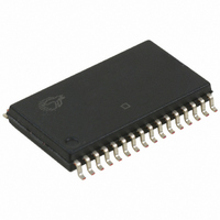
Package Diagrams (continued 0.793[20.142] 0.817[20.751] 0.101[2.565] 0.111[2.819] 0.050[1.270] BSC. 0.014[0.355] 0.020[0.508] Document #: 38-10001 Rev. *G Figure 13. 32-Pin (450-Mil) SOIC S32.45 1 DIMENSIONS IN INCHES[MM] PACKAGE WEIGHT 1.42gms 0.546[13.868] 0.566[14.376] 0.440[11.176] 0.450[11.430] 32 0.006[0.152] 0.012[0.304] 0.118[2.997] MAX. ...
Page 15
Document History Page Document Title: CY7C53150, CY7C53120 Neuron Chip Network Processor Document Number: 38-10001 Submission REV. ECN NO. Date ** 111472 11/28/01 *A 111990 02/06/02 *B 114465 04/24/02 *C 115269 04/26/02 *D 124450 03/25/03 *E 837840 3/14/07 *F 2811866 11/20/2009 ...
Page 16
... Cypress against all charges. Any Source Code (software and/or firmware) is owned by Cypress Semiconductor Corporation (Cypress) and is protected by and subject to worldwide patent protection (United States and foreign), United States copyright laws and international treaty provisions. Cypress hereby grants to licensee a personal, non-exclusive, non-transferable license to copy, use, modify, create derivative works of, and compile the Cypress Source Code and derivative works for the sole purpose of creating custom software and or firmware in support of licensee product to be used only in conjunction with a Cypress integrated circuit as specified in the applicable agreement ...