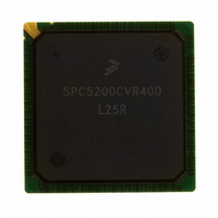
SPC5200CVR400 Freescale Semiconductor, SPC5200CVR400 Datasheet - Page 28

SPC5200CVR400
Manufacturer Part Number
SPC5200CVR400
Description
IC MPU 32BIT 400MHZ 272-PBGA
Manufacturer
Freescale Semiconductor
Datasheet
1.MPC5200CVR400B.pdf
(80 pages)
Specifications of SPC5200CVR400
Processor Type
MPC52xx PowerPC 32-Bit
Speed
400MHz
Voltage
1.5V
Mounting Type
Surface Mount
Package / Case
272-PBGA
Features
-
Available stocks
Company
Part Number
Manufacturer
Quantity
Price
Company:
Part Number:
SPC5200CVR400
Manufacturer:
SUNPLUS
Quantity:
10 037
Company:
Part Number:
SPC5200CVR400
Manufacturer:
Freescale Semiconductor
Quantity:
10 000
Company:
Part Number:
SPC5200CVR400B
Manufacturer:
SEMIKRON
Quantity:
200
Company:
Part Number:
SPC5200CVR400B
Manufacturer:
Freescale Semiconductor
Quantity:
10 000
Part Number:
SPC5200CVR400BL25R
Manufacturer:
FREESCALE
Quantity:
20 000
Company:
Part Number:
SPC5200CVR400BM62CREV1
Manufacturer:
FRRESCAL..
Quantity:
2 831
Company:
Part Number:
SPC5200CVR400BR2
Manufacturer:
Freescale Semiconductor
Quantity:
10 000
Company:
Part Number:
SPC5200CVR400L25R
Manufacturer:
FRRESCAL..
Quantity:
788
Company:
Part Number:
SPC5200CVR400R2
Manufacturer:
Freescale Semiconductor
Quantity:
10 000
Part Number:
SPC5200CVR400R2
Manufacturer:
FREESCALE
Quantity:
20 000
Electrical and Thermal Characteristics
3.3.7
The Local Plus Bus is the external bus interface of the MPC5200. Maximum eight configurable
Chip-selects are provided. There are two main modes of operation: non-MUXed (Legacy and Burst) and
MUXED. The reference clock is the PCI CLK. The maximum bus frequency is 66 MHz.
Definition of Acronyms and Terms:
WS = Wait State
DC = Dead Cycle
LB = Long Burst
DS = Data size in Byte
tPCIck = PCI clock period
tIPBIck = IPBI clock period
3.3.7.1
28
Sym
t
t
CSN
CSA
t
t
t
t
t
t
t
t
t
t
t
t
t
10
11
12
13
3
4
5
6
7
8
9
1
2
PCI CLK to CS assertion
PCI CLK to CS negation
CS pulse width
ADDR valid before CS assertion
ADDR hold after CS negation
OE assertion before CS assertion
OE negation before CS negation
RW valid before CS assertion
RW hold after CS negation
DATA output valid before CS assertion
DATA output hold after CS negation
DATA input setup before CS negation
DATA input hold after CS negation
ACK assertion after CS assertion
ACK negation after CS negation
Local Plus Bus
Non-MUXed Mode
Figure 11. Timing Diagram—IPBI and PCI clock (example ratio: 4:1)
PCI CLK
IPBI CLK
Description
Table 24. Non-MUXed Mode Timing
MPC5200 Data Sheet, Rev. 4
tPCIck
tIPBIck
(2+WS)*t
t
t
t
t
t
t
t
IPBIck
IPBIck
IPBIck
IPBIck
IPBIck
PCIck
PCIck
Min
2.8
0
-
-
-
-
-
PCIck
(2+WS)*t
(DC+1)*t
t
t
Max
PCIck
PCIck
0.4
0.4
1.8
1.8
-
-
-
-
-
-
-
PCIck
PCIck
Units
ns
ns
ns
ns
ns
ns
ns
ns
ns
ns
ns
ns
ns
ns
ns
Freescale Semiconductor
Notes SpecID
1
2
3
3
A7.12
A7.10
A7.11
A7.13
A7.14
A7.15
A7.1
A7.2
A7.3
A7.4
A7.5
A7.6
A7.7
A7.8
A7.9


