SPC5200CVR400 Freescale Semiconductor, SPC5200CVR400 Datasheet - Page 34
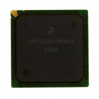
SPC5200CVR400
Manufacturer Part Number
SPC5200CVR400
Description
IC MPU 32BIT 400MHZ 272-PBGA
Manufacturer
Freescale Semiconductor
Datasheet
1.MPC5200CVR400B.pdf
(80 pages)
Specifications of SPC5200CVR400
Processor Type
MPC52xx PowerPC 32-Bit
Speed
400MHz
Voltage
1.5V
Mounting Type
Surface Mount
Package / Case
272-PBGA
Features
-
Available stocks
Company
Part Number
Manufacturer
Quantity
Price
Company:

Part Number:
SPC5200CVR400
Manufacturer:
SUNPLUS
Quantity:
10 037
Company:
Part Number:
SPC5200CVR400
Manufacturer:
Freescale Semiconductor
Quantity:
10 000
Company:
Part Number:
SPC5200CVR400B
Manufacturer:
SEMIKRON
Quantity:
200
Company:
Part Number:
SPC5200CVR400B
Manufacturer:
Freescale Semiconductor
Quantity:
10 000
Part Number:
SPC5200CVR400BL25R
Manufacturer:
FREESCALE
Quantity:
20 000
Company:
Part Number:
SPC5200CVR400BM62CREV1
Manufacturer:
FRRESCAL..
Quantity:
2 831
Company:
Part Number:
SPC5200CVR400BR2
Manufacturer:
Freescale Semiconductor
Quantity:
10 000
Company:
Part Number:
SPC5200CVR400L25R
Manufacturer:
FRRESCAL..
Quantity:
788
Company:
Part Number:
SPC5200CVR400R2
Manufacturer:
Freescale Semiconductor
Quantity:
10 000
Part Number:
SPC5200CVR400R2
Manufacturer:
FREESCALE
Quantity:
20 000


Electrical and Thermal Characteristics
The MPC5200 ATA Host Controller design makes data available coincidentally with the active edge of the
WRITE strobe in PIO and Multiword DMA modes.
All ATA transfers are programmed in terms of system clock cycles (IP bus clocks) in the ATA Host
Controller timing registers. This puts constraints on the ATA protocols and their respective timing modes
in which the ATA Controller can communicate with the drive.
Faster ATA modes (i.e., UDMA 0, 1, 2) are supported when the system is running at a sufficient frequency
to provide adequate data transfer rates. Adequate data transfer rates are a function of the following:
The ATA clock is the same frequency as the IP bus clock in MPC5200. See the MPC5200 User Manual [1].
34
•
•
•
•
•
t2i
tA
tB
t0
t1
t2
t3
t4
t5
t6
t9
Write data is latched by the drive at the inactive edge of the WRITE strobe. This gives ample
setup-time beyond that required by the ATA-4 specification.
Data is held unchanged until the next active edge of the WRITE strobe. This gives ample
hold-time beyond that required by the ATA-4 specification.
The MPC5200 operating frequency (IP bus clock frequency)
Internal MPC5200 bus latencies
Other system load dependent variables
Cycle Time
Address valid to DIOR/DIOW setup
DIOR/DIOW pulse width 16-bit
DIOR/DIOW recovery time
DIOW data setup
DIOW data hold
DIOR data setup
DIOR data hold
DIOR/DIOW to address
valid hold
IORDY setup
IORDY pulse width
8-bit
PIO Timing Parameter
All output timing numbers are specified for nominal 50 pF loads.
Table 27. PIO Mode Timing Specifications
MPC5200 Data Sheet, Rev. 4
Min/Max
(ns)
max
max
min
min
min
min
min
min
min
min
min
min
NOTE
Mode 0
1250
(ns)
600
165
290
70
60
30
50
20
35
—
5
Mode 1
1250
(ns)
383
125
290
50
45
20
35
15
35
—
5
Mode 2
1250
(ns)
240
100
290
30
30
15
20
10
35
—
5
Mode 3
1250
(ns)
180
30
80
80
70
30
10
20
10
35
5
Freescale Semiconductor
Mode 4
1250
(ns)
120
25
70
70
25
20
10
20
10
35
5
SpecID
A8.10
A8.11
A8.1
A8.2
A8.3
A8.4
A8.5
A8.6
A8.7
A8.8
A8.9
Related parts for SPC5200CVR400
Image
Part Number
Description
Manufacturer
Datasheet
Request
R

Part Number:
Description:
Manufacturer:
Freescale Semiconductor, Inc
Datasheet:
Part Number:
Description:
Manufacturer:
Freescale Semiconductor, Inc
Datasheet:
Part Number:
Description:
Manufacturer:
Freescale Semiconductor, Inc
Datasheet:
Part Number:
Description:
Manufacturer:
Freescale Semiconductor, Inc
Datasheet:
Part Number:
Description:
Manufacturer:
Freescale Semiconductor, Inc
Datasheet:
Part Number:
Description:
Manufacturer:
Freescale Semiconductor, Inc
Datasheet:
Part Number:
Description:
Manufacturer:
Freescale Semiconductor, Inc
Datasheet:
Part Number:
Description:
Manufacturer:
Freescale Semiconductor, Inc
Datasheet:
Part Number:
Description:
Manufacturer:
Freescale Semiconductor, Inc
Datasheet:
Part Number:
Description:
Manufacturer:
Freescale Semiconductor, Inc
Datasheet:
Part Number:
Description:
Manufacturer:
Freescale Semiconductor, Inc
Datasheet:
Part Number:
Description:
Manufacturer:
Freescale Semiconductor, Inc
Datasheet:
Part Number:
Description:
Manufacturer:
Freescale Semiconductor, Inc
Datasheet:
Part Number:
Description:
Manufacturer:
Freescale Semiconductor, Inc
Datasheet:
Part Number:
Description:
Manufacturer:
Freescale Semiconductor, Inc
Datasheet: