MC68306EH16B Freescale Semiconductor, MC68306EH16B Datasheet - Page 36
MC68306EH16B
Manufacturer Part Number
MC68306EH16B
Description
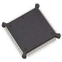
IC MPU INTEGRATED 16MHZ 132-PQFP
Manufacturer
Freescale Semiconductor
Specifications of MC68306EH16B
Processor Type
M683xx 32-Bit
Speed
16MHz
Voltage
5V
Mounting Type
Surface Mount
Package / Case
132-MQFP, 132-PQFP
Controller Family/series
68K
Core Size
32 Bit
Cpu Speed
16.7MHz
No. Of Timers
1
Embedded Interface Type
UART
Digital Ic Case Style
PQFP
Supply Voltage Range
4.75V To 5.25V
Rohs Compliant
Yes
Lead Free Status / RoHS Status
Lead free / RoHS Compliant
Features
-
Available stocks
Company
Part Number
Manufacturer
Quantity
Price
Company:

Part Number:
MC68306EH16B
Manufacturer:
DATEL
Quantity:
87
Company:
Part Number:
MC68306EH16B
Manufacturer:
Freescale Semiconductor
Quantity:
10 000
Company:
Part Number:
MC68306EH16BR2
Manufacturer:
Freescale Semiconductor
Quantity:
10 000


A bus cycle consists of eight states. The various signals are asserted during specific
states of a read cycle as follows:
STATE 0
STATE 1
STATE 2
STATE 3
STATE 4
STATE 5
STATE 6
STATE 7
STATE 5
STATE 6
STATE 7
STATE 8
STATE 9
3.1.2 Write Cycle
During a write cycle, the processor sends bytes of data to the memory or peripheral
device. If the instruction specifies a word or long-word operation, the processor issues
both UDS and LDS and writes both bytes. A long-word write is accomplished by two
consecutive word writes. When the instruction specifies a byte operation, the processor
uses the internal A0 bit to determine which byte to write and issues the appropriate data
3-4
The read cycle starts in state 0 (S0). The processor places valid function
codes on FC0–FC2, a valid address on the bus, and drives R/W high to
identify a read cycle.
On the rising edge of state 2 (S2), the processor asserts AS and
UDS/LDS .
During state 4 (S4), the processor waits for a cycle termination signal
(DTACK or BERR ). If neither termination signal is asserted before the falling
edge at the end of S4, the processor inserts wait states (full clock cycles)
until either DTACK or BERR is asserted.
Case 1: DTACK received, with or without BERR .
driven onto the data bus.
On the falling edge of the clock entering state 7 (S7), the processor latches
data from the addressed device and negates AS and UDS , LDS . The device
negates DTACK or BERR at this time.
Case 2: BERR received without DTACK .
AS and UDS/LDS negated. Slave negates BERR.
During state 1 (S1), no bus signals are altered.
During state 3 (S3), no bus signals are altered.
During state 5 (S5), no bus signals are altered.
Sometime between state 2 (S2) and state 6 (S6), data from the device is
During state 5 (S5), no bus signals are altered.
During state 6 (S6), no bus signals are altered.
During state 7 (S7), no bus signals are altered.
During state 8 (S8), no bus signals are altered.
Freescale Semiconductor, Inc.
For More Information On This Product,
MC68306 USER'S MANUAL
Go to: www.freescale.com
MOTOROLA
Related parts for MC68306EH16B
Image
Part Number
Description
Manufacturer
Datasheet
Request
R

Part Number:
Description:
Manufacturer:
Freescale Semiconductor, Inc
Datasheet:
Part Number:
Description:
Manufacturer:
Freescale Semiconductor, Inc
Datasheet:
Part Number:
Description:
Manufacturer:
Freescale Semiconductor, Inc
Datasheet:
Part Number:
Description:
Manufacturer:
Freescale Semiconductor, Inc
Datasheet:
Part Number:
Description:
Manufacturer:
Freescale Semiconductor, Inc
Datasheet:
Part Number:
Description:
Manufacturer:
Freescale Semiconductor, Inc
Datasheet:
Part Number:
Description:
Manufacturer:
Freescale Semiconductor, Inc
Datasheet:
Part Number:
Description:
Manufacturer:
Freescale Semiconductor, Inc
Datasheet:
Part Number:
Description:
Manufacturer:
Freescale Semiconductor, Inc
Datasheet:
Part Number:
Description:
Manufacturer:
Freescale Semiconductor, Inc
Datasheet:
Part Number:
Description:
Manufacturer:
Freescale Semiconductor, Inc
Datasheet:
Part Number:
Description:
Manufacturer:
Freescale Semiconductor, Inc
Datasheet:
Part Number:
Description:
Manufacturer:
Freescale Semiconductor, Inc
Datasheet:
Part Number:
Description:
Manufacturer:
Freescale Semiconductor, Inc
Datasheet:
Part Number:
Description:
Manufacturer:
Freescale Semiconductor, Inc
Datasheet: