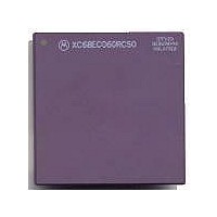
MC68040FE33A Freescale Semiconductor, MC68040FE33A Datasheet - Page 116

MC68040FE33A
Manufacturer Part Number
MC68040FE33A
Description
IC MICROPROCESSOR 32BIT 184-CQFP
Manufacturer
Freescale Semiconductor
Datasheet
1.MC68EC040FE33A.pdf
(442 pages)
Specifications of MC68040FE33A
Processor Type
M680x0 32-Bit
Speed
33MHz
Voltage
5V
Mounting Type
Surface Mount
Package / Case
184-CQFP
Package
184CQFP
Processor Series
M680xx
Core
CPU32
Lead Free Status / RoHS Status
Lead free / RoHS Compliant
Features
-
Lead Free Status / Rohs Status
Details
Available stocks
Company
Part Number
Manufacturer
Quantity
Price
Company:
Part Number:
MC68040FE33A
Manufacturer:
Freescale Semiconductor
Quantity:
10 000
- Current page: 116 of 442
- Download datasheet (4Mb)
The following examples are for PSTx encodings:
5.9.2 Bus Clock (BCLK)
This input signal is used as a reference for all bus timing. It is a TTL-compatible signal and
cannot be gated off. Refer to Section 11 MC68040 Electrical and Thermal
Characteristics for electrical specifications.
5.9.3 Processor Clock (PCLK)—Not on MC68040V and MC68EC040V
PCLK is used to derive all internal timing. This clock is also TTL compatible and cannot be
gated off. Refer to Section 11 MC68040 Electrical and Thermal Characteristics for
electrical specifications.
5.10 MMU DISABLE (
The MMU disable signal dynamically disables the translation of addresses by the MMUs.
The assertion of MDIS does not flush the address translation caches (ATCs); ATC entries
become available again when MDIS is negated. During a processor reset, the level on
MDIS is latched and used to select the normal data latch mode (MDIS high) or DLE mode
(MDIS low). Refer to Section 3 Memory Management Unit (Except MC68EC040 and
MC68EC040V) for a description of address translation and to Section 7 Bus Operation
for information about DLE mode.
5.11 DATA LATCH ENABLE (DLE)—ONLY ON MC68040
This input signal is used in DLE mode to latch the input data bus on read transfers. DLE
mode can be used to support asynchronous memory interfaces by allowing the interface
to specify when data should be latched instead of requiring data to be valid on the rising
edge of BCLK.
5-14
1. An access error terminates an instruction such that the instruction execution stage is
2. An FTRAPcc that does not take an exception ending with the ‘end current
3. Two simultaneous interrupt exception processing sequences follow an ADD
4. An RTE instruction follows an ADD instruction. The ‘end current instruction’ is
not reached. In this case, an ‘end current instruction’ is not indicated. Exception
processing starts, the exception stacking status is indicated, and then the virtual
JMP causes the ‘supervisor, branch taken/end current instruction’ encoding.
instruction’ encoding. The exception stacking status is indicated and then reaches
the ‘supervisor, branch taken/end current instruction’ encoding if the FTRAPcc ends
in an exception.
instruction. The ADD instruction ends with ‘end current instruction’, followed by
exception stacking, followed by ‘branch taken/end current instruction’, followed by
exception stacking, followed by ‘branch taken/end current instruction’.
followed by RTE executing followed by a branch taken/end current instruction.
Freescale Semiconductor, Inc.
MDIS
For More Information On This Product,
)—NOT ON MC68EC040
M68040 USER’S MANUAL
Go to: www.freescale.com
MOTOROLA
Related parts for MC68040FE33A
Image
Part Number
Description
Manufacturer
Datasheet
Request
R

Part Number:
Description:
(MC600 Series) INTEGRATED CIRCUITS
Manufacturer:
ETC
Datasheet:
Part Number:
Description:
Manufacturer:
Freescale Semiconductor, Inc
Datasheet:
Part Number:
Description:
Manufacturer:
Freescale Semiconductor, Inc
Datasheet:
Part Number:
Description:
Manufacturer:
Freescale Semiconductor, Inc
Datasheet:
Part Number:
Description:
Manufacturer:
Freescale Semiconductor, Inc
Datasheet:
Part Number:
Description:
Manufacturer:
Freescale Semiconductor, Inc
Datasheet:
Part Number:
Description:
Manufacturer:
Freescale Semiconductor, Inc
Datasheet:
Part Number:
Description:
Manufacturer:
Freescale Semiconductor, Inc
Datasheet:
Part Number:
Description:
Manufacturer:
Freescale Semiconductor, Inc
Datasheet:
Part Number:
Description:
Manufacturer:
Freescale Semiconductor, Inc
Datasheet:
Part Number:
Description:
Manufacturer:
Freescale Semiconductor, Inc
Datasheet:
Part Number:
Description:
Manufacturer:
Freescale Semiconductor, Inc
Datasheet:
Part Number:
Description:
Manufacturer:
Freescale Semiconductor, Inc
Datasheet:
Part Number:
Description:
Manufacturer:
Freescale Semiconductor, Inc
Datasheet:
Part Number:
Description:
Manufacturer:
Freescale Semiconductor, Inc
Datasheet:


