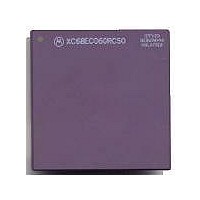
MC68040FE33A Freescale Semiconductor, MC68040FE33A Datasheet - Page 152

MC68040FE33A
Manufacturer Part Number
MC68040FE33A
Description
IC MICROPROCESSOR 32BIT 184-CQFP
Manufacturer
Freescale Semiconductor
Datasheet
1.MC68EC040FE33A.pdf
(442 pages)
Specifications of MC68040FE33A
Processor Type
M680x0 32-Bit
Speed
33MHz
Voltage
5V
Mounting Type
Surface Mount
Package / Case
184-CQFP
Package
184CQFP
Processor Series
M680xx
Core
CPU32
Lead Free Status / RoHS Status
Lead free / RoHS Compliant
Features
-
Lead Free Status / Rohs Status
Details
Available stocks
Company
Part Number
Manufacturer
Quantity
Price
Company:
Part Number:
MC68040FE33A
Manufacturer:
Freescale Semiconductor
Quantity:
10 000
- Current page: 152 of 442
- Download datasheet (4Mb)
7.4.1 Byte, Word, and Long-Word Read Transfers
During a read transfer, the processor receives data from a memory or peripheral device.
Since the data read for a byte, word, or long-word access is not placed in either of the
internal caches by definition, the processor ignores the level on the transfer cache inhibit
(TCI) signal when latching the data. The bus controller performs byte, word, and long-word
read transfers for the following cases:
Figure 7-8 is a flowchart for byte, word, and long-word read transfers. Bus operations are
similar for each case and vary only with the size indicated and the portion of the data bus
used for the transfer. Figure 7-9 is a functional timing diagram for byte, word, and long-
word read transfers.
7-10
• Accesses to a disabled cache.
• Accesses to a memory page that is specified noncachable.
• Accesses that are implicitly noncachable (read-modify-write accesses and accesses
• Accesses that do not allocate in the data cache on a read miss (table searches,
• The first transfer of a line read is terminated with transfer burst inhibit (TBI), forcing
to an alternate logical address space via the MOVES instruction).
exception vector fetches, and exception stack deallocation for an RTE instruction).
completion of the line access using three additional long-word read transfers.
1) SET R/W TO READ
2) DRIVE ADDRESS ON A31–A0
3) DRIVE USER PAGE ATTRIBUTES ON UPA1, UPA0
4) DRIVE SIZE ON SIZ1, SIZ0 (BYTE, WORD,
5) DRIVE TRANSFER TYPE ON TT1, TT0
6) DRIVE TRANSFER MODIFIER ON TM2–TM0
7) CIOUT BECOMES VALID
8) ASSERT TS FOR ONE CLOCK
9) ASSERT TIP
1) LATCH DATA
OR LONG WORD)
Figure 7-8. Byte, Word, and Long-Word Read Transfer Flowchart
START NEXT CYCLE
ADDRESS DEVICE
ACQUIRE DATA
PROCESSOR
Freescale Semiconductor, Inc.
For More Information On This Product,
M68040 USER’S MANUAL
Go to: www.freescale.com
1) DECODE ADDRESS
2) PLACE DATA ON APPROPRIATE BYTES OF
3) ASSERT TA
1) REMOVE DATA FROM D31–D0
2) NEGATE TA
D31–D0 BASED ON SIZEx, A0, AND A1
EXTERNAL DEVICE
TERMINATE CYCLE
PRESENT DATA
MOTOROLA
Related parts for MC68040FE33A
Image
Part Number
Description
Manufacturer
Datasheet
Request
R

Part Number:
Description:
(MC600 Series) INTEGRATED CIRCUITS
Manufacturer:
ETC
Datasheet:
Part Number:
Description:
Manufacturer:
Freescale Semiconductor, Inc
Datasheet:
Part Number:
Description:
Manufacturer:
Freescale Semiconductor, Inc
Datasheet:
Part Number:
Description:
Manufacturer:
Freescale Semiconductor, Inc
Datasheet:
Part Number:
Description:
Manufacturer:
Freescale Semiconductor, Inc
Datasheet:
Part Number:
Description:
Manufacturer:
Freescale Semiconductor, Inc
Datasheet:
Part Number:
Description:
Manufacturer:
Freescale Semiconductor, Inc
Datasheet:
Part Number:
Description:
Manufacturer:
Freescale Semiconductor, Inc
Datasheet:
Part Number:
Description:
Manufacturer:
Freescale Semiconductor, Inc
Datasheet:
Part Number:
Description:
Manufacturer:
Freescale Semiconductor, Inc
Datasheet:
Part Number:
Description:
Manufacturer:
Freescale Semiconductor, Inc
Datasheet:
Part Number:
Description:
Manufacturer:
Freescale Semiconductor, Inc
Datasheet:
Part Number:
Description:
Manufacturer:
Freescale Semiconductor, Inc
Datasheet:
Part Number:
Description:
Manufacturer:
Freescale Semiconductor, Inc
Datasheet:
Part Number:
Description:
Manufacturer:
Freescale Semiconductor, Inc
Datasheet:


