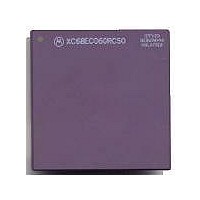
MC68040FE33A Freescale Semiconductor, MC68040FE33A Datasheet - Page 210

MC68040FE33A
Manufacturer Part Number
MC68040FE33A
Description
IC MICROPROCESSOR 32BIT 184-CQFP
Manufacturer
Freescale Semiconductor
Datasheet
1.MC68EC040FE33A.pdf
(442 pages)
Specifications of MC68040FE33A
Processor Type
M680x0 32-Bit
Speed
33MHz
Voltage
5V
Mounting Type
Surface Mount
Package / Case
184-CQFP
Package
184CQFP
Processor Series
M680xx
Core
CPU32
Lead Free Status / RoHS Status
Lead free / RoHS Compliant
Features
-
Lead Free Status / Rohs Status
Details
Available stocks
Company
Part Number
Manufacturer
Quantity
Price
Company:
Part Number:
MC68040FE33A
Manufacturer:
Freescale Semiconductor
Quantity:
10 000
- Current page: 210 of 442
- Download datasheet (4Mb)
Freescale Semiconductor, Inc.
7.11 SPECIAL MODES OF OPERATION
The MC68LC040 and MC68EC040 do not support the following three modes of operation,
which for the M68040 are selectively enabled during processor reset and remain in effect
until the next processor reset. Refer to Appendix A MC68LC040 and Appendix B
MC68EC040 for differences in the special modes of operation for the MC68LC040 and
MC68EC040.
7.11.1 Output Buffer Impedance Selection
All output drivers in the M68040 can be configured to operate in either a large buffer mode
(low-impedance driver) or small buffer mode (high-impedance driver). Large buffers have
a nominal output impedance of 6
for both high and low drive, resulting in minimum
output delays. Signal traces driven by large buffers usually require transmission line
effects to be considered in their design, including the use of signal termination. Small
buffers have a nominal impedance of 25
for high and low drive, resulting in longer
output delays and less critical board-design requirements. Refer to Section 11 MC68040
Electrical and Thermal Characteristics for further information on electrical
specifications, buffer characteristics, and transmission line design examples. The output
drivers are configured in three groups. Each group of signals is configured depending on
the corresponding IPL≈ signal level during processor reset (see Table 5-5).
7.11.2 Multiplexed Bus Mode
The multiplexed bus mode changes the timing of the three-state control logic for the
address and data buses to support generation of a multiplexed address/data bus. When
the M68040 is operating in this mode, the address and data bus signals can be hardwired
together to form a single 32-bit bus, with address and data information time-multiplexed on
the bus. This configuration minimizes the number of pins required to interface to
peripheral devices without requiring additional discrete multiplexing logic. This mode is
enabled during a processor reset by a logic zero on the CDIS signal.
Figure 7-46 illustrates a line write with multiplexed bus mode enabled. The address bus
drivers are enabled during C1 and disabled during C2. Later in C2, the data bus drivers
are enabled to drive the data bus with the data to be written. The address bus is only
driven for the BCLK rising edge at the start of each bus cycle.
7-68
M68040 USER’S MANUAL
MOTOROLA
For More Information On This Product,
Go to: www.freescale.com
Related parts for MC68040FE33A
Image
Part Number
Description
Manufacturer
Datasheet
Request
R

Part Number:
Description:
(MC600 Series) INTEGRATED CIRCUITS
Manufacturer:
ETC
Datasheet:
Part Number:
Description:
Manufacturer:
Freescale Semiconductor, Inc
Datasheet:
Part Number:
Description:
Manufacturer:
Freescale Semiconductor, Inc
Datasheet:
Part Number:
Description:
Manufacturer:
Freescale Semiconductor, Inc
Datasheet:
Part Number:
Description:
Manufacturer:
Freescale Semiconductor, Inc
Datasheet:
Part Number:
Description:
Manufacturer:
Freescale Semiconductor, Inc
Datasheet:
Part Number:
Description:
Manufacturer:
Freescale Semiconductor, Inc
Datasheet:
Part Number:
Description:
Manufacturer:
Freescale Semiconductor, Inc
Datasheet:
Part Number:
Description:
Manufacturer:
Freescale Semiconductor, Inc
Datasheet:
Part Number:
Description:
Manufacturer:
Freescale Semiconductor, Inc
Datasheet:
Part Number:
Description:
Manufacturer:
Freescale Semiconductor, Inc
Datasheet:
Part Number:
Description:
Manufacturer:
Freescale Semiconductor, Inc
Datasheet:
Part Number:
Description:
Manufacturer:
Freescale Semiconductor, Inc
Datasheet:
Part Number:
Description:
Manufacturer:
Freescale Semiconductor, Inc
Datasheet:
Part Number:
Description:
Manufacturer:
Freescale Semiconductor, Inc
Datasheet:


