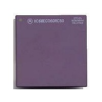
MC68040FE33A Freescale Semiconductor, MC68040FE33A Datasheet - Page 407

MC68040FE33A
Manufacturer Part Number
MC68040FE33A
Description
IC MICROPROCESSOR 32BIT 184-CQFP
Manufacturer
Freescale Semiconductor
Datasheet
1.MC68EC040FE33A.pdf
(442 pages)
Specifications of MC68040FE33A
Processor Type
M680x0 32-Bit
Speed
33MHz
Voltage
5V
Mounting Type
Surface Mount
Package / Case
184-CQFP
Package
184CQFP
Processor Series
M680xx
Core
CPU32
Lead Free Status / RoHS Status
Lead free / RoHS Compliant
Features
-
Lead Free Status / Rohs Status
Details
Available stocks
Company
Part Number
Manufacturer
Quantity
Price
Company:
Part Number:
MC68040FE33A
Manufacturer:
Freescale Semiconductor
Quantity:
10 000
- Current page: 407 of 442
- Download datasheet (4Mb)
The test logic also includes an instruction shift register and two test data registers, a
boundary scan register and a bypass register. The boundary scan register links all device
signal pins into a chain that can be controlled by the 3-bit instruction shift register.
C.6.1 Instruction Shift Register
The MC68040V and MC68EC040V IEEE standard 1149.1A implementations include a 3-
bit instruction shift register without parity. The register shifts one of six instructions, which
can either select the test to be performed or access a test data register, or both. Data is
transferred from the instruction shift register to latched decoded outputs during the
update-IR state. The instruction shift register is reset to all ones in the TAP controller test-
logic-reset state, which is equivalent to selecting the BYPASS instruction. During the
capture-IR state, the binary value 001 is loaded into the parallel inputs of the instruction
shift register.
The MC68040V and MC68EC040V IEEE standard 1149.1A implementations include three
mandatory standard public instructions (BYPASS, SAMPLE/PRELOAD, and EXTEST),
two optional public standard instructions, and one manufacturer's private instruction. The
five public instructions provide the capability to disable all device output drivers, operate
the device in a BYPASS configuration, and conduct boundary scan test operations. Table
C-3 lists the three bits used in the instruction shift register to decode the instructions and
MOTOROLA
TDI—A test data input with an internal pullup resistor sampled on the rising edge of
TDO—A three-state test data output actively driven only in the shift-IR and shift-DR
TCK.
Figure C-4. MC68040V and MC68EC040V Test Logic Block Diagram
controller states that changes on the falling edge of TCK.
TMS
TCK
TDI
Freescale Semiconductor, Inc.
For More Information On This Product,
187
188-BIT BOUNDARY SCAN REGISTER
BYPASS
2
Go to: www.freescale.com
3-BIT INSTRUCTION SHIFT REGISTER
M68040 USER’S MANUAL
TEST DATA REGISTERS
LATCHED DECODER
0
0
TDO
C-11
Related parts for MC68040FE33A
Image
Part Number
Description
Manufacturer
Datasheet
Request
R

Part Number:
Description:
(MC600 Series) INTEGRATED CIRCUITS
Manufacturer:
ETC
Datasheet:
Part Number:
Description:
Manufacturer:
Freescale Semiconductor, Inc
Datasheet:
Part Number:
Description:
Manufacturer:
Freescale Semiconductor, Inc
Datasheet:
Part Number:
Description:
Manufacturer:
Freescale Semiconductor, Inc
Datasheet:
Part Number:
Description:
Manufacturer:
Freescale Semiconductor, Inc
Datasheet:
Part Number:
Description:
Manufacturer:
Freescale Semiconductor, Inc
Datasheet:
Part Number:
Description:
Manufacturer:
Freescale Semiconductor, Inc
Datasheet:
Part Number:
Description:
Manufacturer:
Freescale Semiconductor, Inc
Datasheet:
Part Number:
Description:
Manufacturer:
Freescale Semiconductor, Inc
Datasheet:
Part Number:
Description:
Manufacturer:
Freescale Semiconductor, Inc
Datasheet:
Part Number:
Description:
Manufacturer:
Freescale Semiconductor, Inc
Datasheet:
Part Number:
Description:
Manufacturer:
Freescale Semiconductor, Inc
Datasheet:
Part Number:
Description:
Manufacturer:
Freescale Semiconductor, Inc
Datasheet:
Part Number:
Description:
Manufacturer:
Freescale Semiconductor, Inc
Datasheet:
Part Number:
Description:
Manufacturer:
Freescale Semiconductor, Inc
Datasheet:


