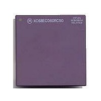
MC68040FE33A Freescale Semiconductor, MC68040FE33A Datasheet - Page 412

MC68040FE33A
Manufacturer Part Number
MC68040FE33A
Description
IC MICROPROCESSOR 32BIT 184-CQFP
Manufacturer
Freescale Semiconductor
Datasheet
1.MC68EC040FE33A.pdf
(442 pages)
Specifications of MC68040FE33A
Processor Type
M680x0 32-Bit
Speed
33MHz
Voltage
5V
Mounting Type
Surface Mount
Package / Case
184-CQFP
Package
184CQFP
Processor Series
M680xx
Core
CPU32
Lead Free Status / RoHS Status
Lead free / RoHS Compliant
Features
-
Lead Free Status / Rohs Status
Details
Available stocks
Company
Part Number
Manufacturer
Quantity
Price
Company:
Part Number:
MC68040FE33A
Manufacturer:
Freescale Semiconductor
Quantity:
10 000
- Current page: 412 of 442
- Download datasheet (4Mb)
All MC68040V and MC68EC040V bidirectional pins include two boundary scan data cells,
an input, and an output. One of five associated boundary scan control cells controls each
bidirectional pin. If these cells contain a logic one, the associated bidirectional or three-
state pin will be configured as an output and enabled. The cell captures the current value
during the capture-DR state. All five control cells are reset (i.e., logic zero) in the test-
logic-reset state. The five bidirectional/three-state control cells, their boundary scan
register bit positions, and the 188 boundary scan bit definitions are not currently available.
C.6.3 Restrictions
Control over the output enable signals using the boundary scan register and the EXTEST
and HIGHZ instructions requires a compatible circuit-board test environment to avoid
destructive configurations. The user is responsible for avoiding situations in which the
MC68040V and MC68EC040V output drivers are enabled into actively driven networks.
The MC68040V and MC68EC040V include on-chip circuitry to detect the initial application
of power to the device. Power-on reset (POR, which is an internal signal), the output of
this circuitry, is used to reset both the system and the IEEE 1149.1A logic. The purpose of
applying POR to the IEEE 1149.1A circuitry is to avoid the possibility of bus contention
during power-on. The time required to complete device power-on is power supply
dependent. However, the TAP controller remains in the test-logic-reset state while POR is
asserted. The TAP controller does not respond to user commands until POR is negated.
The following restrictions apply:
C.6.4 Disabling The IEEE Standard 1149.1A Operation
There are two considerations for non-IEEE standard 1149.1A operation. First, TCK does
not include an internal pullup resistor and should not be left unconnected to preclude mid-
level inputs. The second consideration is to ensure that the IEEE standard 1149.1A test
logic remains transparent to the system logic by providing the ability to force the test-logic-
reset state. Figure C-10 illustrates a circuit to disable the IEEE standard 1149.1A test logic
for the MC68040V and MC68EC040V.
C-16
1. Leaving the TAP controller test-logic-reset state negates the ability to achieve the
2. The TCK input is not blocked in LPSTOP mode. To consume minimal power, the
3. The TMS and TDI pins include on-chip pull-up resistors. In LPSTOP mode, these
4. The external system must assert RSTI within eight bus clocks of exiting from the
lowest power consumption during the LPSTOP instruction, but does not otherwise
affect device functionality.
TCK input should be externally connected to V CC or ground.
two pins should remain either connected to V CC or ground to achieve minimal
power consumption.
EXTEST JTAG instruction or else on the tenth bus clock, the MC68040V and
MC68EC040V will begin normal reset processing.
Freescale Semiconductor, Inc.
For More Information On This Product,
M68040 USER’S MANUAL
Go to: www.freescale.com
MOTOROLA
Related parts for MC68040FE33A
Image
Part Number
Description
Manufacturer
Datasheet
Request
R

Part Number:
Description:
(MC600 Series) INTEGRATED CIRCUITS
Manufacturer:
ETC
Datasheet:
Part Number:
Description:
Manufacturer:
Freescale Semiconductor, Inc
Datasheet:
Part Number:
Description:
Manufacturer:
Freescale Semiconductor, Inc
Datasheet:
Part Number:
Description:
Manufacturer:
Freescale Semiconductor, Inc
Datasheet:
Part Number:
Description:
Manufacturer:
Freescale Semiconductor, Inc
Datasheet:
Part Number:
Description:
Manufacturer:
Freescale Semiconductor, Inc
Datasheet:
Part Number:
Description:
Manufacturer:
Freescale Semiconductor, Inc
Datasheet:
Part Number:
Description:
Manufacturer:
Freescale Semiconductor, Inc
Datasheet:
Part Number:
Description:
Manufacturer:
Freescale Semiconductor, Inc
Datasheet:
Part Number:
Description:
Manufacturer:
Freescale Semiconductor, Inc
Datasheet:
Part Number:
Description:
Manufacturer:
Freescale Semiconductor, Inc
Datasheet:
Part Number:
Description:
Manufacturer:
Freescale Semiconductor, Inc
Datasheet:
Part Number:
Description:
Manufacturer:
Freescale Semiconductor, Inc
Datasheet:
Part Number:
Description:
Manufacturer:
Freescale Semiconductor, Inc
Datasheet:
Part Number:
Description:
Manufacturer:
Freescale Semiconductor, Inc
Datasheet:


