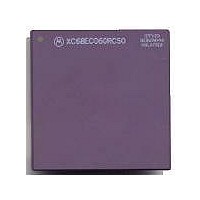
MC68040FE33A Freescale Semiconductor, MC68040FE33A Datasheet - Page 53

MC68040FE33A
Manufacturer Part Number
MC68040FE33A
Description
IC MICROPROCESSOR 32BIT 184-CQFP
Manufacturer
Freescale Semiconductor
Datasheet
1.MC68EC040FE33A.pdf
(442 pages)
Specifications of MC68040FE33A
Processor Type
M680x0 32-Bit
Speed
33MHz
Voltage
5V
Mounting Type
Surface Mount
Package / Case
184-CQFP
Package
184CQFP
Processor Series
M680xx
Core
CPU32
Lead Free Status / RoHS Status
Lead free / RoHS Compliant
Features
-
Lead Free Status / Rohs Status
Details
Available stocks
Company
Part Number
Manufacturer
Quantity
Price
Company:
Part Number:
MC68040FE33A
Manufacturer:
Freescale Semiconductor
Quantity:
10 000
- Current page: 53 of 442
- Download datasheet (4Mb)
0 of an address loaded into the URP or the SRP must be zero. Transfers of data to and
from these 32-bit registers are long-word transfers.
3.1.2 Translation Control Register
The 16-bit TCR contains two control bits to enable paged address translation and to select
page size. The operating system must flush the ATCs before enabling address translation
since the TCR accesses and reset do not flush the ATCs. All unimplemented bits of this
register are read as zeros and must always be written as zeros. The M68040 always uses
word transfers to access this 16-bit register. The fields of the TCRs are defined following
Figure 3-4, which illustrates the TCR.
E—Enable
P—Page Size
3-4
31
This bit enables and disables paged address translation.
A reset operation clears this bit. When translation is disabled, logical addresses are
used as physical addresses. The MMU instruction, PFLUSH, can be executed
successfully despite the state of the E-bit. PTEST results are undefined if the MMU is
disabled and no table search occurs. If translation is disabled and an access does not
match a transparent translation register (TTR), the access has the following default
attributes on the TTR: the caching mode is cachable/write-through, write protection is
disabled, and the user attribute signals (UPA1 and UPA0) are zero.
This bit selects the memory page size.
A reset operation does not affect this bit. The bit must be initialized after a reset.
0 = Disable
1 = Enable
0 = 4 Kbytes
1 = 8 Kbytes
NOTE: Bits 13–0 are undefined (reserved).
15
E
Figure 3-4. Translation Control Register Format
SUPERVISOR ROOT POINTER
Figure 3-3. URP and SRP Register Formats
14
P
USER ROOT POINTER
Freescale Semiconductor, Inc.
13
0
For More Information On This Product,
12
0
11
0
M68040 USER'S MANUAL
Go to: www.freescale.com
10
0
9
0
8
0
7
0
6
0
5
0
4
0
9
3
0
8
0
0
2
0
0
0
1
0
0
0
0
0
0
0
0
0
0
0
MOTOROLA
0
0
0
0
0
0
0
Related parts for MC68040FE33A
Image
Part Number
Description
Manufacturer
Datasheet
Request
R

Part Number:
Description:
(MC600 Series) INTEGRATED CIRCUITS
Manufacturer:
ETC
Datasheet:
Part Number:
Description:
Manufacturer:
Freescale Semiconductor, Inc
Datasheet:
Part Number:
Description:
Manufacturer:
Freescale Semiconductor, Inc
Datasheet:
Part Number:
Description:
Manufacturer:
Freescale Semiconductor, Inc
Datasheet:
Part Number:
Description:
Manufacturer:
Freescale Semiconductor, Inc
Datasheet:
Part Number:
Description:
Manufacturer:
Freescale Semiconductor, Inc
Datasheet:
Part Number:
Description:
Manufacturer:
Freescale Semiconductor, Inc
Datasheet:
Part Number:
Description:
Manufacturer:
Freescale Semiconductor, Inc
Datasheet:
Part Number:
Description:
Manufacturer:
Freescale Semiconductor, Inc
Datasheet:
Part Number:
Description:
Manufacturer:
Freescale Semiconductor, Inc
Datasheet:
Part Number:
Description:
Manufacturer:
Freescale Semiconductor, Inc
Datasheet:
Part Number:
Description:
Manufacturer:
Freescale Semiconductor, Inc
Datasheet:
Part Number:
Description:
Manufacturer:
Freescale Semiconductor, Inc
Datasheet:
Part Number:
Description:
Manufacturer:
Freescale Semiconductor, Inc
Datasheet:
Part Number:
Description:
Manufacturer:
Freescale Semiconductor, Inc
Datasheet:


