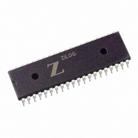
Z0840004PSC Zilog, Z0840004PSC Datasheet - Page 97

Z0840004PSC
Manufacturer Part Number
Z0840004PSC
Description
IC 4MHZ Z80 NMOS CPU 40-DIP
Manufacturer
Zilog
Datasheet
1.Z0840004PSC.pdf
(98 pages)
Specifications of Z0840004PSC
Processor Type
Z80
Features
NMOS
Speed
4MHz
Voltage
5V
Mounting Type
Through Hole
Package / Case
40-DIP (0.620", 15.75mm)
Lead Free Status / RoHS Status
Contains lead / RoHS non-compliant
Available stocks
Company
Part Number
Manufacturer
Quantity
Price
Company:
Part Number:
Z0840004PSC
Manufacturer:
ZILOG
Quantity:
2 000
Part Number:
Z0840004PSC
Manufacturer:
ZILOG
Quantity:
20 000
Part Number:
Z0840004PSC (Z80CPU)
Manufacturer:
ZILOG
Quantity:
20 000
Part Number:
Z0840004PSC(Z80CPU)
Manufacturer:
ZILOG
Quantity:
20 000
ZiLOG
ZAC03-0004
TERM
SDE:
SEM:
SIMS:
SL-Lot:
SPC:
STS:
Silicon:
Soft bake:
SOIC:
Source:
Spec. Limit:
Spin:
Sputtering:
TD:
TDDB:
TEM:
THB:
TSOP:
Test patterns:
Thermal oxide:
UL:
DEFINITION
Statistical Design of Experiments.
Scanning Electron Microscope. A microscope which makes use of
a scanning beam of electrons to image detail less than 100A in size
(surface only).
Secondary Ion Mass Spectroscopy.
Special Lot. ZiLOG identification used to identify products
designed to unique customer requirements.
Statistical Process Control.
Ship-to-Stock. Eliminates need for customer IQC.
Metallic element which forms the substrate in most semiconductor
devices.
A step preparing freshly spun photoresist for exposure by baking it
in an oven (to remove excess solvent).
Small Outline Integrated Circuit package.
Equivalent to the drain of a transistor with the exception that
electrons leave the source into the channel of the active device.
Absolute acceptable limit for a process parameter.
A process step which coats a spinning wafer with liquid photoresist
by dispensing the liquid onto its center.
Deposition of a metal layer by bombarding a metal target with
heavy ions from a gaseous (e.g., argon) plasma. Metal atoms are
removed from the target and deposited onto the wafer during this
process.
Technology Development.
Time Dependent Dielectric Breakdown.
Transmission Electron Microscope. A microscope used to obtain
high-resolution images with a transmitted electron beam by
electron lens imaging rather than scanning.
Temperature Humidity Bias (85°C/85% RH).
Thin small outline package.
Special electrical test structures included on production device
wafers for monitoring critical parameters.
A high quality Si
furnace (as opposed to externally deposited glass).
Underwriters Laboratory.
O2
layer grown by oxidizing the silicon in a
2002 Quality and Reliability Report
11- 8


