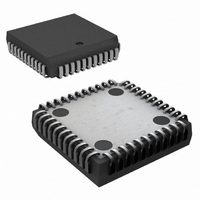
TP3094V/NOPB National Semiconductor, TP3094V/NOPB Datasheet

TP3094V/NOPB
Specifications of TP3094V/NOPB
*TP3094V/NOPB
TP3094V
Available stocks
Related parts for TP3094V/NOPB
TP3094V/NOPB Summary of contents
Page 1
... AGND0 17 VXI0 ® ® COMBO and TRI-STATE are registered trademarks of National Semiconductor Corporation © 2000 National Semiconductor Corporation Features • Handles four voice channels • Complete Codec and Filter system including: - Transmit and receive channel filters - A-law or -law companding encoder/decoder • Power down mode for low power consumption • ...
Page 2
Simplified Block Diagram GXO0 VXI0- - ADC + VRO0 DAC GXO1 - VXI1- ADC + VRO1 DAC GXO2 VXI2- - ADC + VRO2 DAC GXO3 VXI3- - ADC + VRO3 DAC Digital Signal Processor FIGURE 1. Simplified block diagram 2 ...
Page 3
Pin Descriptions MCLK (input) Master and PCM bit clock input. Must be either 1.536MHz/1.544MHz, 2.048MHz, 4.096MHz or 8.192MHz. Its value is automatically detected in- ternally on power up with the valid frame sync in- put. AVCC0, AVCC1 Positive supply pins ...
Page 4
Pin Descriptions (continued) expects its individual transmit and receive frame signal. When it is HIGH, the 32 bit mode is select- ed; in this mode FSX0 and FSR0 are used as framing signals and the TS are allocated consec- utively ...
Page 5
When both the transmit and receive frame sync of a channel are missing the channel will go into Power Down Mode (if only one of them is missing the channel will not go into Power Down). A max- imum of ...
Page 6
Functional Description (continued) 8-bit Mode In the 8-bit mode, PCM data is transferred inde- pendently for each of the four channels. Each channel has its dedicated transmit and receive frame signals, which determine the time-slots to be taken on the ...
Page 7
Functional Description (continued) bypassing the low frequency filter. Test Modes Normal Operation Single Channel Digital Loopback Single Channel Analog Loopback Single Channel DC Conversion 4 Channels Digital Loopback 4 Channels Analog Loopback 4 Channels DC Conversion Invalid States Where A0, ...
Page 8
Timing Diagrams MCLK FSX3 or FSR3 FSX2 or FSR2 FSX0 or FSR0 D7 CH3 CH3 D0 DR TSX FIGURE 2. Timing diagram for PCM Interface, 8-bit mode (Long Frame Sync MCLK TSX t DBTS MCLK ...
Page 9
Timing Diagrams (continued) MCLK FSX3 or FSR3 FSX2 or FSR2 FSX0 or FSR0 D7 CH3 D0 DX CH3 TSX FIGURE 5. Timing diagram for PCM Interface, 8-bit mode (Short Frame Sync) TSX t DBTS MCLK 1st 2nd ...
Page 10
Timing Diagrams (continued) MCLK FSX0 or FSR0 FSX1 or FSR1 D7 CH0 D0 D7 CH1 CH0 D0 D7 CH1 D0 D7 TSX FIGURE 7. Timing diagram for PCM Interface, 32-bit mode TSX t DBTS MCLK ...
Page 11
... Absolute Maximum Ratings If Military/Aerospace specified devices are required, please contact the National Semiconductor Sales Office/Dis- tributors for availability and specifications DGND CC Voltage at any digital inputs or outputs Voltage at any analog inputs or outputs Storage temperature range Lead temperature(Soldering, 10 Sec) ESD (human body model) ...
Page 12
Electrical Characteristics Symbol Parameter Power Dissipation I 0 Power down current (all CC channels down Power up active current CC (all channel active) Amplitude Response Absolute Levels t Virtual decision value max defined per ITU G.711 G Transmit ...
Page 13
Electrical Characteristics Symbol Parameter G Receive gain variation RAL with level Note 2: Measure voiceband image signal, stimulus signal level is -25dBm0. Distortion STD Transmit signal to total XP distortion SFD Transmit single fre- X quency distortion STD Receive signal ...
Page 14
Electrical Characteristics Symbol Parameter Envelope delay distortion D Transmit delay, absolute XA D Transmit delay, relative Receive delay, absolute RA D Receive delay, relative Noise N Transmit Idle channel XP noise, ...
Page 15
Electrical Characteristics Symbol Parameter Crosstalk CT Receive to transmit R-X crosstalk (Intra-channel Crosstalk) CTFE Far end crosstalk with X analog stimulus (Inter- channel crosstalk) CTNE Near end crosstalk with X digital stimulus (Inter- channel crosstalk) CT Transmit to receive X-R ...
Page 16
Timing Specifications Symbol Parameter Clock and Data Timing All timing parameters are measured at V 1/t Frequency of MCLK PM DC MCLK Duty Cycle MCLK t Rise time of MCLK RM t Fall time of MCLK FM t Setup time ...
Page 17
Applications Information Tip SLIC Ring Tip SLIC Ring Tip SLIC Ring Tip SLIC Ring FIGURE 9. Typical application in a non cascaded mode System Bus +5V Supply AVCC0 AVCC1 DVCC GX0 DX DR VXI0 Zb FSX0 FSR0 VRO0 T PDN0 ...
Page 18
Applications Information Tip SLIC Ring Tip SLIC Ring Tip SLIC Ring Tip SLIC Ring Tip SLIC Ring Tip SLIC Ring Tip SLIC Ring Tip SLIC Ring FIGURE 10. TP3094 in a cascade mode +5V Supply AVCC0 AVCC1 DVCC GX0 DX ...
Page 19
... A critical component is any component of a life sup- port device or system whose failure to perform can be reasonably expected to cause the failure of the life support device or system affect its safety or ef- National Semiconductor National Semiconductor Europe Asia Pacific Customer Response Group Fax: (+49) 0-180-530 85 86 Tel: 65-254-4466 Email: europe ...


