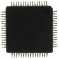
ISP1362BDFA ST-Ericsson Inc, ISP1362BDFA Datasheet - Page 112

ISP1362BDFA
Manufacturer Part Number
ISP1362BDFA
Description
IC USB OTG CONTROLLER 64-LQFP
Manufacturer
ST-Ericsson Inc
Datasheet
1.ISP1362EEUM.pdf
(153 pages)
Specifications of ISP1362BDFA
Controller Type
USB 2.0 Controller
Interface
Parallel/Serial
Voltage - Supply
3 V ~ 3.6 V
Operating Temperature
-40°C ~ 85°C
Mounting Type
Surface Mount
Package / Case
64-LQFP
Lead Free Status / RoHS Status
Lead free / RoHS Compliant
Current - Supply
-
Other names
568-1219
ISP1362BD,151
ISP1362BD-S
ISP1362BD,151
ISP1362BD-S
Available stocks
Company
Part Number
Manufacturer
Quantity
Price
Company:
Part Number:
ISP1362BDFA
Manufacturer:
STE
Quantity:
5
NXP Semiconductors
ISP1362_5
Product data sheet
Bit
Symbol
Reset
Access
15.1.5 DcInterruptEnable register (R/W: C3h/C2h)
DAKOLY
R/W
7
0
Table 116. DcHardwareConfiguration register: bit description
This command is used to individually enable or disable interrupts from all endpoints, as
well as interrupts caused by events on the USB bus (SOF, EOT, suspend, resume, reset).
A bus reset will not change any of the programmed bit values.
Bit
15
14
13
12
11 to 8
7
6
5
4
3
2
1
0
DRQPOL
R/W
6
1
Symbol
-
EXTPUL
NOLAZY
CLKRUN
CKDIV[3:0]
DAKOLY
DRQPOL
DAKPOL
-
WKUPCS
-
INTLVL
INTPOL
DAKPOL
R/W
5
0
Description
reserved
Logic 1 indicates that an external 1.5 k pull-up resistor is used on
pin OTG_DP1 (in device mode) and that SoftConnect is not used. Bus
reset value: unchanged.
Logic 1 disables output on pin CLKOUT of the LazyClock frequency
(115 kHz
to switch to LazyClock output after approximately 2 ms delay, following the
setting of bit GOSUSP of the DcMode register. Bus reset value:
unchanged.
Logic 1 indicates that internal clocks are always running, even during the
‘suspend’ state. Logic 0 switches off the internal oscillator and PLL, when
they are not needed. During the ‘suspend’ state, this bit must be made
logic 0 to meet suspend current requirements. The clock is stopped after a
delay of approximately 2 ms, following the setting of bit GOSUSP of the
DcMode register. Bus reset value: unchanged.
This field specifies clock division factor N, which controls the clock
frequency on output CLKOUT pin. The output frequency in MHz is given
by
15), with a reset value of 12 MHz (N = 3). The hardware design
guarantees no glitches during frequency change. Bus reset value:
unchanged.
Logic 1 selects DACK-only DMA mode. Logic 0 selects 8237 compatible
DMA mode. Bus reset value: unchanged.
Selects the DREQ2 pin signal polarity (0 = active LOW; 1 = active HIGH).
Bus reset value: unchanged.
Selects the DACK2 pin signal polarity (0 = active LOW; 1 = active HIGH).
Bus reset value: unchanged.
reserved
Logic 1 enables remote wake-up using a LOW level on input CS. Bus reset
value: unchanged.
reserved
Selects interrupt signaling mode on output (0 = level; 1 = pulsed). In
pulsed mode, an interrupt produces 166 ns pulse. Bus reset value:
unchanged.
Selects the INT2 signal polarity (0 = active LOW; 1 = active HIGH). Bus
reset value: unchanged.
Rev. 05 — 8 May 2007
48
N
reserved
+
50 %) during the suspend state. Logic 0 causes pin CLKOUT
4
0
-
1
. The clock frequency range is 3 MHz to 48 MHz (N = 0 to
WKUPCS
R/W
3
0
reserved
Single-chip USB OTG Controller
R/W
2
1
INTLVL
R/W
1
0
© NXP B.V. 2007. All rights reserved.
ISP1362
INTPOL
111 of 152
R/W
0
0


