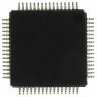
ISP1362BDFA ST-Ericsson Inc, ISP1362BDFA Datasheet - Page 14

ISP1362BDFA
Manufacturer Part Number
ISP1362BDFA
Description
IC USB OTG CONTROLLER 64-LQFP
Manufacturer
ST-Ericsson Inc
Datasheet
1.ISP1362EEUM.pdf
(153 pages)
Specifications of ISP1362BDFA
Controller Type
USB 2.0 Controller
Interface
Parallel/Serial
Voltage - Supply
3 V ~ 3.6 V
Operating Temperature
-40°C ~ 85°C
Mounting Type
Surface Mount
Package / Case
64-LQFP
Lead Free Status / RoHS Status
Lead free / RoHS Compliant
Current - Supply
-
Other names
568-1219
ISP1362BD,151
ISP1362BD-S
ISP1362BD,151
ISP1362BD-S
Available stocks
Company
Part Number
Manufacturer
Quantity
Price
Company:
Part Number:
ISP1362BDFA
Manufacturer:
STE
Quantity:
5
NXP Semiconductors
8. Host and device bus interface
Table 3.
[1]
ISP1362_5
Product data sheet
Priority CS
1
2
3
4
5
Only to enable and disable the bus. Depends only on the DACK signal.
L
L
H
H
H
Bus access priority table for the ISP1362
7.10 Charge pump
A1
L
H
X
X
X
7.9 GoodLink
Indication of a good USB connection is provided through the GoodLink technology
(open-drain, maximum current: 4 mA). During enumeration, LED indicators momentarily
blink on corresponding to the enumeration traffic of the ISP1362 ports. The LED also
blinks on whenever there is valid traffic to the USB ports. In ‘suspend’ mode, the LED is
off.
This feature of GoodLink provides a user-friendly indication on the status of the USB
traffic between the host and the hub, as well as the connected devices. It is a useful
diagnostics tool to isolate faulty equipment, and helps to reduce field support and hotline
costs.
The charge pump generates a 5 V supply from 3.3 V to drive V
an A-device in OTG mode. For details, see
The interface between the external microprocessor and the ISP1362 Host Controller (HC)
and Peripheral Controller is separately handled by the individual bus interface circuitry.
The host or device automultiplex selects the path for the host access or the device access.
This selection is determined by the A1 address line. For any access to the Host Controller
or Peripheral Controller registers, the command phase and the data phase are needed,
which is determined by the A0 address line.
All the functionality of the ISP1362 can be accessed using a group of registers and two
buffer memory areas (one for the Host Controller and the other for the Peripheral
Controller). Registers can be accessed using Programmed I/O (PIO) mode. The buffer
memory can be accessed using both PIO and Direct Memory Access (DMA) modes.
When CS is LOW (active), address pin A1 has priority over DREQ and DACK. Therefore,
as long as the CS pin is held LOW, the ISP1362 bus interface does not respond to any
DACK signals. When CS is HIGH (inactive), the bus interface will respond to DREQn and
DACKn. Address pin A1 will be ignored when CS is inactive.
An active DACKn signal when DREQn is inactive will be ignored. If DREQ1, DACK1,
DREQ2 and DACK2 are active, the bus interface will be switched off to avoid potential
data corruption.
Table 3
DACK1
X
X
L
X
X
provides the bus access priority for the ISP1362.
DACK2
X
X
X
L
X
DREQ1
X
X
H
L
H
Rev. 05 — 8 May 2007
DREQ2
X
X
L
H
H
Host Controller and Peripheral Controller active
Host Controller
Peripheral Controller
Host Controller
Peripheral Controller
no driving
Section
10.6.
Single-chip USB OTG Controller
[1]
[1]
BUS
when the ISP1362 is
© NXP B.V. 2007. All rights reserved.
ISP1362
13 of 152


