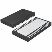
LTC4269CDKD-1#PBF Linear Technology, LTC4269CDKD-1#PBF Datasheet - Page 16

LTC4269CDKD-1#PBF
Manufacturer Part Number
LTC4269CDKD-1#PBF
Description
IC PD/OPTO FLYBACK CTRLR 32-DFN
Manufacturer
Linear Technology
Type
Power Over Ethernet (PoE)r
Datasheet
1.LTC4269IDKD-1PBF.pdf
(44 pages)
Specifications of LTC4269CDKD-1#PBF
Applications
Power Interface Switch for Power Over Ethernet (PoE) Devices
Voltage - Supply
14 V ~ 16 V
Operating Temperature
0°C ~ 70°C
Mounting Type
Surface Mount
Package / Case
32-DFN
Current - Supply
1.35mA
Interface
IEEE 802.3af
Controller Type
Powered Device Interface Controller (PD)
Input Voltage
60V
Supply Current
6.4mA
Digital Ic Case Style
DFN
No. Of Pins
32
Duty Cycle (%)
88%
Frequency
100kHz
Operating Temperature Range
0°C To +70°C
Msl
MSL 1 - Unlimited
Rohs Compliant
Yes
Operating Temperature (max)
70C
Operating Temperature (min)
0C
Pin Count
32
Mounting
Surface Mount
Package Type
DFN EP
Case Length
7mm
Screening Level
Commercial
Lead Free Status / RoHS Status
Lead free / RoHS Compliant
Available stocks
Company
Part Number
Manufacturer
Quantity
Price
LTC4269-1
To control the power-on surge currents in the system, the
LTC4269-1 provides a fi xed inrush current, allowing C1 to
ramp up to the line voltage in a controlled manner.
The LTC4269-1 keeps the PD inrush current below the
PSE current limit to provide a well controlled power-up
characteristic that is independent of the PSE behavior.
This ensures a PD using the LTC4269-1 interoperability
with any PSE.
TURN-ON/ TURN-OFF THRESHOLD
The IEEE 802.3af/at specifi cation for the PD dictates a
maximum turn-on voltage of 42V and a minimum turn-off
voltage of 30V. This specifi cation provides an adequate
voltage to begin PD operation, and to discontinue PD op-
eration when the input voltage is too low. In addition, this
specifi cation allows PD designs to incorporate an ON/OFF
hysteresis window to prevent start-up oscillations.
The LTC4269-1 features an ON/OFF hysteresis window (see
Figure 5) that conforms with the IEEE 802.3af/at specifi ca-
tion and accommodates the voltage drop in the cable and
input diode bridge at the onset of the inrush current.
Once C1 is fully charged, the LTC4269-1 turns on is internal
MOSFET and passes power to the PD load. The LTC4269-1
continues to power the PD load as long as the input voltage
APPLICATIONS INFORMATION
16
PSE
TO
Figure 5. LTC4269-1 ON/OFF and Overvoltage Lockout
V
LTC4269-1
PORTN
V
VOLTAGE
0V TO ON*
>ON*
<OFF*
>OVLO
*INCLUDES ON/OFF HYSTERESIS
ON THRESHOLD 36.1V
OFF THRESHOLD 30.7V
OVLO THRESHOLD 71.0V
PORTP
OVERVOLTAGE
ON/OFF AND
LOCKOUT
CIRCUIT
– V
PORTN
POWER MOSFET
LTC4269-1
OFF
OFF
OFF
ON
V
PORTP
V
NEG
CURRENT-LIMITED
TURN ON
+
42691 F05
C1
5μF
MIN
LOAD
PD
does not fall below the OFF threshold. When the LTC4269-1
input voltage falls below the OFF threshold, the PD load
is disconnected, and classifi cation mode resumes. C1
discharges through the LTC4269-1 circuitry.
COMPLEMENTARY POWER GOOD
When LTC4269-1 fully charges the load capacitor (C1),
power good is declared and the LTC4269-1 load can safely
begin operation. The LTC4269-1 provides complementary
power good signals that remain active during normal op-
eration and are de-asserted when the input voltage falls
below the OFF threshold, when the input voltage exceeds
the overvoltage lockout (OVLO) threshold, or in the event
of a thermal shutdown (see Figure 6).
The PWRGD pin features an open collector output refer-
enced to V
pin. When power good is declared and active, the PWRGD
pin is high impedance with respect to V
14V clamp limits the PWRGD pin voltage. Connecting the
PWRGD pin to the UVLO prevents the DC/DC converter
Figure 6. LTC4269-1 Power Good Functional and State Diagram
V
V
PORTN
PORTN
5
6
LTC4269-1
NEG
ON/OFF
OVLO
BOLD LINE INDICATES HIGH CURRENT PATH
which can interface directly with the UVLO
TSD
POWER
GOOD
AND NOT IN THERMAL SHUTDOWN
NOT
OR THERMAL SHUTDOWN
CONTROL
CIRCUIT
ON < V
INRUSH COMPLETE
V
V
PORTP
PORTP
PORTP
> OVLO
< OFF
< OVLO
POWER
GOOD
NEG
42691 F06
. An internal
30
29
27
26
PWRGD
PWRGD
V
V
NEG
NEG
42691fb


