AD9951YSVZ Analog Devices Inc, AD9951YSVZ Datasheet - Page 14
AD9951YSVZ
Manufacturer Part Number
AD9951YSVZ
Description
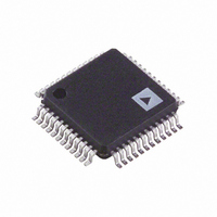
IC DDS DAC 14BIT 1.8V 48-TQFP
Manufacturer
Analog Devices Inc
Specifications of AD9951YSVZ
Resolution (bits)
14 b
Master Fclk
400MHz
Tuning Word Width (bits)
32 b
Voltage - Supply
1.71 V ~ 1.96 V
Operating Temperature
-40°C ~ 105°C
Mounting Type
Surface Mount
Package / Case
48-TQFP Exposed Pad, 48-eTQFP, 48-HTQFP, 48-VQFP
Data Rate
25Mbps
Rf Ic Case Style
TQFP
No. Of Pins
48
Supply Voltage Range
1.8V To 3.3V
Operating Temperature Range
-40°C To +105°C
Msl
MSL 3 - 168 Hours
Ic Function
Direct Digital Synthesizer
Digital Ic Case Style
TQFP
Svhc
No SVHC (15-Dec-2010)
Rohs Compliant
Yes
Termination Type
SMD
Ic Generic Number
9951
Base Number
9951
Filter Terminals
SMD
Lead Free Status / RoHS Status
Lead free / RoHS Compliant
For Use With
AD9951/PCB - BOARD EVAL FOR AD9951
Lead Free Status / Rohs Status
Compliant
Available stocks
Company
Part Number
Manufacturer
Quantity
Price
Company:

Part Number:
AD9951YSVZ
Manufacturer:
AD
Quantity:
1 300
Company:
Part Number:
AD9951YSVZ
Manufacturer:
ADI
Quantity:
102
Company:
Part Number:
AD9951YSVZ
Manufacturer:
ADI
Quantity:
650
Company:
Part Number:
AD9951YSVZ
Manufacturer:
Analog Devices Inc
Quantity:
10 000


AD9951
Table 5. Register Map
Register
Name
(Serial
Address)
Register No.
Scale Factor
Offset Word
Ramp Rate
Amplitude
Amplitude
Frequency
Function
Function
Register
2 (CFR2)
Control
Control
(POW0)
Tuning
(FTW0)
(CFR1)
(0x00)
(0x01)
(0x02)
(0x03)
(0x04)
(0x05)
Phase
(ARR)
(ASF)
Word
No.1
Bit
Range
<23:16>
<31:24>
<23:16>
<23:16>
<31:24>
<15:8>
<15:8>
<15:8>
<15:8>
<15:8>
<7:0>
<7:0>
<7:0>
<7:0>
<7:0>
<7:0>
(MSB)
Bit 7
Automatic
Auto Ramp Rate Speed
Not Used
Power-
Enable
Digital
Down
Sync
Not Used<1:0>
Control <1:0>
0x00 or 0x01, or 0x02 or 0x03: Bypass Multiplier
0x04 to 0x14: 4× to 20× Multiplication
Bit 6
Not Used
Not Used
Software
Manual
Sync
Not Used
REFCLK Multiplier
Bit 5
Not Used
AutoClr
Power-
Accum
Down
Phase
DAC
Amplitude Scale Factor Register <7:0>
Frequency Tuning Word No. 0 <23:16>
Frequency Tuning Word No. 0 <31:24>
Amplitude Ramp Rate Register <7:0>
Frequency Tuning Word No. 0 <15:8>
Frequency Tuning Word No. 0 <7:0>
Rev. A | Page 14 of 28
Phase Offset Word No. 0 <7:0>
Bit 4
Enable SINE
Clock Input
Output
Power-
Down
Amplitude Scale Factor Register <13:8>
Not Used
Phase Offset Word No. 0 <13:8>
Bit 3
Not Used
External
Power-
Down
Enable
Mode
Speed
High
Sync
Not Used
Bit 2
Load ARR
Hardware
Not Used
@ I/O UD
Accum.
Manual
Enable
Range
Phase
Clear
Sync
VCO
Bit 1
SYNC_CLK
Charge Pump Current
CRYSTAL
OUT Pin
Disable
Enable
Active
Input
SDIO
Only
OSK
Out
<1:0>
(LSB)
Bit 0
LSB First
Keying
Used
Auto
Used
OSK
Not
Not
Default
Value
0x00
0x00
0x00
0x00
0x00
0x00
0x18
0x00
0x00
0x00
0x00
0x00
0x00
0x00
0x00
0x00
Related parts for AD9951YSVZ
Image
Part Number
Description
Manufacturer
Datasheet
Request
R

Part Number:
Description:
BOARD EVAL FOR AD9951
Manufacturer:
Analog Devices Inc
Datasheet:
Part Number:
Description:
BOARD EVALUATION FOR AD9851
Manufacturer:
Analog Devices Inc
Datasheet:


Part Number:
Description:
±1.7g Dual-Axis IMEMS Accelerometer Evaluation Board
Manufacturer:
Analog Devices Inc
Datasheet:
Part Number:
Description:
Inertial Sensor Evaluation System
Manufacturer:
Analog Devices Inc
Datasheet:
Part Number:
Description:
Manufacturer:
Analog Devices Inc
Datasheet:
Part Number:
Description:
Manufacturer:
Analog Devices Inc
Datasheet:
Part Number:
Description:
Manufacturer:
Analog Devices Inc
Datasheet:
Part Number:
Description:
Manufacturer:
Analog Devices Inc
Datasheet:
Part Number:
Description:
Manufacturer:
Analog Devices Inc
Datasheet:
Part Number:
Description:
Manufacturer:
Analog Devices Inc
Datasheet:
Part Number:
Description:
Manufacturer:
Analog Devices Inc
Datasheet:
Part Number:
Description:
Manufacturer:
Analog Devices Inc
Datasheet: