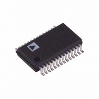
AD9850BRSZ Analog Devices Inc, AD9850BRSZ Datasheet - Page 5

AD9850BRSZ
Manufacturer Part Number
AD9850BRSZ
Description
IC DDS SYNTHESIZER CMOS 28-SSOP
Manufacturer
Analog Devices Inc
Datasheet
1.AD9850BRSZ-REEL.pdf
(20 pages)
Specifications of AD9850BRSZ
Mounting Type
Surface Mount
Resolution (bits)
10 b
Master Fclk
125MHz
Tuning Word Width (bits)
32 b
Voltage - Supply
3.3V, 5V
Operating Temperature
-40°C ~ 85°C
Package / Case
28-SSOP
Rf Ic Case Style
SSOP
No. Of Pins
28
Supply Voltage Range
4.75V To 5.25V, 3.3V
Operating Temperature Range
-40°C To +85°C
Msl
MSL 3 - 168 Hours
Frequency Max
125MHz
Current Rating
30A
Frequency
125MHz
Rohs Compliant
Yes
Lead Free Status / RoHS Status
Lead free / RoHS Compliant
Pin
No.
4 to 1,
28 to 25
5, 24
6, 23
7
8
9
10, 19
11, 18
12
13
14
15
16
17
20
21
22
REV. H
Mnemonic
D0 to D7
DGND
DVDD
W_CLK
FQ_UD
CLKIN
AGND
AVDD
R
QOUTB
QOUT
VINN
VINP
DACBL (NC) DAC Baseline. This is the DAC baseline voltage reference; this lead is internally bypassed and should
IOUTB
IOUT
RESET
SET
Function
8-Bit Data Input. This is the 8-bit data port for iteratively loading the 32-bit frequency and the 8-bit phase/
control word. D7 = MSB; D0 = LSB. D7 (Pin 25) also serves as the input pin for the 40-bit serial data-word.
Digital Ground. These are the ground return leads for the digital circuitry.
Supply Voltage Leads for Digital Circuitry.
Word Load Clock. This clock is used to load the parallel or serial frequency/phase/control words.
Frequency Update. On the rising edge of this clock, the DDS updates to the frequency (or phase)
loaded in the data input register; it then resets the pointer to Word 0.
Reference Clock Input. This may be a continuous CMOS-level pulse train or sine input biased at
1/2 V supply. The rising edge of this clock initiates operation.
Analog Ground. These leads are the ground return for the analog circuitry (DAC and comparator).
Supply Voltage for the Analog Circuitry (DAC and Comparator).
DAC’s External R
normal applications (F
relationship is I
Output Complement. This is the comparator’s complement output.
Output True. This is the comparator’s true output.
Inverting Voltage Input. This is the comparator’s negative input.
Noninverting Voltage Input. This is the comparator’s positive input.
normally be considered a no connect for optimum performance.
Complementary Analog Output of the DAC.
Analog Current Output of the DAC.
Reset. This is the master reset function; when set high, it clears all registers (except the input register), and
the DAC output goes to cosine 0 after additional clock cycles—see Figure 7.
OUT
Table I. PIN FUNCTION DESCRIPTIONS
SET
= 32 (1.248 V/R
Connection. This resistor value sets the DAC full-scale output current. For
S
I
OUT
LSB D0
W CLK
QOUTB
FQ UD
CLKIN
DGND
AGND
QOUT
PIN CONFIGURATION
DVDD
AVDD
R
SET
D3
D2
D1
= 10 mA), the value for R
10
11
12
13
14
NC = NO CONNECT
1
2
3
4
5
6
7
8
9
(Not to Scale)
AD9850
TOP VIEW
SET
–5–
).
28
27
26
25
24
22
23
21
20
19
18
17
16
15
D4
D5
D6
D7 MSB/SERIAL LOAD
DGND
DVDD
RESET
IOUT
IOUTB
AGND
AVDD
DACBL (NC)
VINP
VINN
SET
is 3.9 kΩ connected to ground. The R
AD9850
SET
/I
OUT


