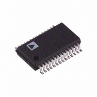
AD9850BRSZ Analog Devices Inc, AD9850BRSZ Datasheet - Page 9

AD9850BRSZ
Manufacturer Part Number
AD9850BRSZ
Description
IC DDS SYNTHESIZER CMOS 28-SSOP
Manufacturer
Analog Devices Inc
Datasheet
1.AD9850BRSZ-REEL.pdf
(20 pages)
Specifications of AD9850BRSZ
Mounting Type
Surface Mount
Resolution (bits)
10 b
Master Fclk
125MHz
Tuning Word Width (bits)
32 b
Voltage - Supply
3.3V, 5V
Operating Temperature
-40°C ~ 85°C
Package / Case
28-SSOP
Rf Ic Case Style
SSOP
No. Of Pins
28
Supply Voltage Range
4.75V To 5.25V, 3.3V
Operating Temperature Range
-40°C To +85°C
Msl
MSL 3 - 168 Hours
Frequency Max
125MHz
Current Rating
30A
Frequency
125MHz
Rohs Compliant
Yes
Lead Free Status / RoHS Status
Lead free / RoHS Compliant
AD9850 is a sampled signal, its output spectrum follows the
Nyquist sampling theorem. Specifically, its output spectrum
contains the fundamental plus aliased signals (images) that
occur at multiples of the reference clock frequency ± the
selected output frequency. A graphical representation of the
sampled spectrum, with aliased images, is shown in Figure 5.
In this example, the reference clock is 100 MHz and the output
frequency is set to 20 MHz. As can be seen, the aliased images
are very prominent and of a relatively high energy level as deter-
mined by the sin(x)/x roll-off of the quantized D/A converter
output. In fact, depending on the fo/reference clock relation-
ship, the first aliased image can be on the order of –3 dB below
the fundamental. A low-pass filter is generally placed between
the output of the D/A converter and the input of the com-
parator to further suppress the effects of aliased images. Obvi-
ously, consideration must be given to the relationship of the
selected output frequency and the reference clock frequency
to avoid unwanted (and unexpected) output anomalies.
To apply the AD9850 as a clock generator, limit the selected
output frequency to <33% of reference clock frequency, and
thereby avoid generating aliased signals that fall within, or close
to, the output band of interest (generally dc-selected output fre-
quency). This practice eases the complexity (and cost) of the
external filter requirement for the clock generator application.
The reference clock frequency of the AD9850 has a minimum
limitation of 1 MHz. The device has internal circuitry that
senses when the minimum clock rate threshold has been exceeded
REV. H
FUNDAMENTAL
20MHz
Figure 5. Output Spectrum of a Sampled Signal
f
OUT
1ST IMAGE
80MHz
REFERENCE CLOCK
fc – fo
sin(x)/x ENVELOPE
FREQUENCY
100MHz
fc
TUNING WORD SPECIFIES
2ND IMAGE
AS A FRACTION OF REF
OUTPUT FREQUENCY
fc + fo
120MHz
CLOCK FREQUENCY
N
Figure 4. Basic DDS Block Diagram and Signal Flow of AD9850
3RD IMAGE
180MHz
2fc – fo
x=( )fo/fc
ACCUMULATOR
CLOCK
PHASE
REF
4TH IMAGE
2fc + fo
220MHz
DDS CIRCUITRY
5TH IMAGE
IN DIGITAL DOMAIN
3fc – fo
280MHz
AMPLITUDE/COS
ALGORITHM
CONV.
–9–
and automatically places itself in the power-down mode. When
in this state, if the clock frequency again exceeds the threshold,
the device resumes normal operation. This shutdown mode
prevents excessive current leakage in the dynamic registers of
the device.
The D/A converter output and comparator inputs are available
as differential signals that can be flexibly configured in any
manner desired to achieve the objectives of the end system. The
typical application of the AD9850 is with single-ended output/
input analog signals, a single low-pass filter, and the generation
of the comparator reference midpoint from the differential DAC
output as shown in Figure 1.
Programming the AD9850
The AD9850 contains a 40-bit register that is used to program the
32-bit frequency control word, the 5-bit phase modulation word,
and the power-down function. This register can be loaded in a
parallel or serial mode.
In the parallel load mode, the register is loaded via an 8-bit bus;
the full 40-bit word requires five iterations of the 8-bit word.
The W_CLK and FQ_UD signals are used to address and load
the registers. The rising edge of FQ_UD loads the (up to) 40-bit
control data-word into the device and resets the address pointer
to the first register. Subsequent W_CLK rising edges load the
8-bit data on words [7:0] and move the pointer to the next
register. After five loads, W_CLK edges are ignored until either
a reset or an FQ_UD rising edge resets the address pointer to
the first register.
In serial load mode, subsequent rising edges of W_CLK shift
the 1-bit data on Pin 25 (D7) through the 40 bits of program-
ming information. After 40 bits are shifted through, an FQ_UD
pulse is required to update the output frequency (or phase).
The function assignments of the data and control words are
shown in Table III; the detailed timing sequence for updating
the output frequency and/or phase, resetting the device, and
powering up/down, are shown in the timing diagrams of
Figures 6 through 12.
Note: There are specific control codes, used for factory test
purposes, that render the AD9850 temporarily inoperable. The
user must take deliberate precaution to avoid inputting the
codes listed in Table II.
CONVERTER
D/A
COS (x)
LP
COMPARATOR
CLK
OUT
AD9850


