MC7808ACT Fairchild Semiconductor, MC7808ACT Datasheet
MC7808ACT
Specifications of MC7808ACT


Related parts for MC7808ACT


MC7808ACT Summary of contents
Page 1
MC7800, MC7800A, NCV7805 1.0 A Positive Voltage Regulators These voltage regulators are monolithic integrated circuits designed as fixed- voltage regulators for a wide variety of applications including local, on-card regulation. These regulators employ internal current limiting, thermal shutdown, and safe-area ...
Page 2
MC7800, MC7800A, NCV7805 MC7800 LAT Q17 R18 100 k Q7 QNPN Q5 QNPN 2 R17 9 QNPN 2 R11 QNPN Zener R1 10. QNPN R2 1. 4.5 k Q14 QNPN ...
Page 3
ELECTRICAL CHARACTERISTICS Characteristic Output Voltage (T = 25°C) J Output Voltage (5.0 mA ≤ I ≤ 1 7.0 Vdc ≤ V ≤ 20 Vdc in 8.0 Vdc ≤ V ≤ 20 Vdc in Line Regulation (Note ...
Page 4
ELECTRICAL CHARACTERISTICS Characteristic Output Voltage (T = 25°C) J Output Voltage (5.0 mA ≤ I ≤ 1 7.5 Vdc ≤ V ≤ 20 Vdc in Line Regulation (Note 4) 7.5 Vdc ≤ V ≤ 25 Vdc, ...
Page 5
ELECTRICAL CHARACTERISTICS Characteristic Output Voltage (T = 25°C) J Output Voltage (5.0 mA ≤ I ≤ 1 8.0 Vdc ≤ V ≤ 21 Vdc in 9.0 Vdc ≤ V ≤ 21 Vdc in Line Regulation, T ...
Page 6
ELECTRICAL CHARACTERISTICS Characteristic Output Voltage (T = 25°C) J Output Voltage (5.0 mA ≤ I ≤ 1 8.6 Vdc ≤ V ≤ 21 Vdc in Line Regulation (Note 8) 8.6 Vdc ≤ V ≤ 25 Vdc, ...
Page 7
ELECTRICAL CHARACTERISTICS Characteristic Output Voltage (T = 25°C) J Output Voltage (5.0 mA ≤ I ≤ 1 10.5 Vdc ≤ V ≤ 23 Vdc in 11.5 Vdc ≤ V ≤ 23 Vdc in Line Regulation, T ...
Page 8
ELECTRICAL CHARACTERISTICS Characteristic Output Voltage (T = 25°C) J Output Voltage (5.0 mA ≤ I ≤ 1 10.6 Vdc ≤ V ≤ 23 Vdc in Line Regulation (Note 12) 10.6 Vdc ≤ V ≤ 25 Vdc, ...
Page 9
ELECTRICAL CHARACTERISTICS Characteristic Output Voltage (T = 25°C) J Output Voltage (5.0 mA ≤ I ≤ 1 11.5 Vdc ≤ V ≤ 24 Vdc in Line Regulation 25°C (Note 14 Vdc ≤ ...
Page 10
ELECTRICAL CHARACTERISTICS Characteristic Output Voltage (T = 25°C) J Output Voltage (5.0 mA ≤ I ≤ 1 11.5 Vdc ≤ V ≤ 24 Vdc in Line Regulation (Note 15) 11.5 Vdc ≤ V ≤ 26 Vdc, ...
Page 11
ELECTRICAL CHARACTERISTICS Characteristic Output Voltage (T = 25°C) J Output Voltage (5.0 mA ≤ I ≤ 1 14.5 Vdc ≤ V ≤ 27 Vdc in 15.5 Vdc ≤ V ≤ 27 Vdc in Line Regulation, T ...
Page 12
ELECTRICAL CHARACTERISTICS Characteristic Output Voltage (T = 25°C) J Output Voltage (5.0 mA ≤ I ≤ 1 14.8 Vdc ≤ V ≤ 27 Vdc in Line Regulation (Note 19) 14.8 Vdc ≤ V ≤ 30 Vdc, ...
Page 13
ELECTRICAL CHARACTERISTICS Characteristic Output Voltage (T = 25°C) J Output Voltage (5.0 mA ≤ I ≤ 1 17.5 Vdc ≤ V ≤ 30 Vdc in 18.5 Vdc ≤ V ≤ 30 Vdc in Line Regulation, T ...
Page 14
ELECTRICAL CHARACTERISTICS Characteristic Output Voltage (T = 25°C) J Output Voltage (5.0 mA ≤ I ≤ 1 17.9 Vdc ≤ V ≤ 30 Vdc in Line Regulation (Note 23) 17.9 Vdc ≤ V ≤ 30 Vdc, ...
Page 15
ELECTRICAL CHARACTERISTICS Characteristic Output Voltage (T = 25°C) J Output Voltage (5.0 mA ≤ I ≤ 1 Vdc ≤ V ≤ 33 Vdc in 22 Vdc ≤ V ≤ 33 Vdc in Line Regulation, (Note ...
Page 16
ELECTRICAL CHARACTERISTICS Characteristic Output Voltage (T = 25°C) J Output Voltage (5.0 mA ≤ I ≤ 1 Vdc ≤ V ≤ 33 Vdc in Line Regulation (Note 27) 21 Vdc ≤ V ≤ 33 Vdc, ...
Page 17
ELECTRICAL CHARACTERISTICS Characteristic Output Voltage (T = 25°C) J Output Voltage (5.0 mA ≤ I ≤ 1 Vdc ≤ V ≤ 38 Vdc in 28 Vdc ≤ V ≤ 38 Vdc in Line Regulation, (Note ...
Page 18
ELECTRICAL CHARACTERISTICS Characteristic Output Voltage (T = 25°C) J Output Voltage (5.0 mA ≤ I ≤ 1 27.3 Vdc ≤ V ≤ 38 Vdc in Line Regulation (Note 31) 27 Vdc ≤ V ≤ 38 Vdc, ...
Page 19
T = -40°C J 2.5 2.0 1 85° 125°C 0 4.0 6.0 8 INPUT/OUTPUT VOLTAGE DIFFERENTIAL (V) in out Figure 2. Peak Output Current ...
Page 20
Design Considerations The MC7800 Series of fixed voltage regulators are designed with Thermal Overload Protection that shuts down the circuit when subjected to an excessive power overload condition, Internal Short Circuit Protection that limits the maximum current the circuit will ...
Page 21
5°C 8.0 = 15°C/W HS 4.0 No Heatsink 0 -50 - AMBIENT TEMPERATURE (°C) A Figure 12. Worst Case Power Dissipation versus Ambient ...
Page 22
Line Regulation - The change in output voltage for a change in the input voltage. The measurement is made under conditions of low dissipation or by using pulse techniques such that the average chip temperature is not significantly affected. Load ...
Page 23
ORDERING INFORMATION Device Nominal Voltage MC7805BT MC7805BTG NCV7805BD2T* NCV7805BD2TG* NCV7805BD2TR4* NCV7805BD2TR4G* NCV7805BT* NCV7805BTG* MC7805CD2T MC7805CD2TG MC7805CD2TR4 MC7805CD2TR4G MC7805CDT MC7805CDTG MC7805CDTRK MC7805CDTRKG MC7805CT MC7805CTG MC7806ACT MC7806ACTG MC7806BD2T MC7806BD2TG MC7806BD2TR4 MC7806BD2TR4G MC7806BT MC7806BTG MC7806CT MC7806CTG †For information on tape and reel specifications, ...
Page 24
... ORDERING INFORMATION Device Nominal Voltage MC7808ABD2T MC7808ABD2TG MC7808ABD2TR4 MC7808ABD2TR4G MC7808ABT MC7808ABTG MC7808ACT MC7808ACTG MC7808BD2T MC7808BD2TG MC7808BD2TR4 MC7808BD2TR4G MC7808BDT MC7808BDTG MC7808BDTRK MC7808BDTRKG MC7808BT MC7808BTG MC7808CD2T MC7808CD2TG MC7808CD2TR4 MC7808CD2TR4G MC7808CDT MC7808CDTG MC7808CDTRK MC7808CDTRKG MC7808CT MC7808CTG †For information on tape and reel specifications, including part orientation and tape sizes, please refer to our Tape and Reel Packaging Specifications Brochure, BRD8011/D ...
Page 25
ORDERING INFORMATION Device Nominal Voltage MC7809ACT MC7809ACTG MC7809BT MC7809BTG MC7809CD2T MC7809CD2TG MC7809CD2TR4 MC7809CD2TR4G MC7809CT MC7809CTG MC7812ABD2T MC7812ABD2TG MC7812ABD2TR4 MC7812ABD2TR4G MC7812ABT MC7812ABTG MC7812ACD2T MC7812ACD2TG MC7812ACD2TR4 MC7812ACD2TR4G MC7812ACT MC7812ACTG MC7812BD2T MC7812BD2TG MC7812BD2TR4 MC7812BD2TR4G MC7812BDT MC7812BDTG †For information on tape and reel specifications, ...
Page 26
ORDERING INFORMATION Device Nominal Voltage MC7812BDTRK MC7812BDTRKG MC7812BT MC7812BTG NCV7812BD2T * NCV7812BD2TR4 * NCV7812BD2TR4G * NCV7812BT * NCV7812BTG * MC7812CD2T MC7812CD2TG MC7812CD2TR4 MC7812CD2TR4G MC7812CDT MC7812CDTG MC7812CDTRK MC7812CDTRKG MC7812CT MC7812CTG †For information on tape and reel specifications, including part orientation and ...
Page 27
ORDERING INFORMATION Device Nominal Voltage MC7815ABD2T MC7815ABD2TG MC7815ABD2TR4 MC7815ABD2TR4G MC7815ABT MC7815ABTG MC7815ACD2T MC7815ACD2TG MC7815ACT MC7815ACTG MC7815BD2T MC7815BD2TG †For information on tape and reel specifications, including part orientation and tape sizes, please refer to our Tape and Reel Packaging Specifications Brochure, ...
Page 28
ORDERING INFORMATION Device Nominal Voltage MC7815BD2TR4 MC7815BD2TR4G MC7815BDT MC7815BDTG MC7815BDTRK MC7815BDTRKG MC7815BT MC7815BTG MC7815CD2T MC7815CD2TG MC7815CD2TR4 MC7815CD2TR4G MC7815CDT MC7815CDTG MC7815CDTRK MC7815CDTRKG MC7815CT MC7815CTG MC7818ACT MC7818ACTG MC7818BT MC7818BTG MC7818CD2T MC7818CD2TR4 MC7818CD2TR4G MC7818CT MC7818CTG †For information on tape and reel specifications, including ...
Page 29
ORDERING INFORMATION Device Nominal Voltage MC7824ACT MC7824ACTG MC7824BD2T MC7824BD2TG MC7824BD2TR4 MC7824BD2TR4G MC7824BT MC7824BTG MC7824CD2T MC7824CD2TG MC7824CD2TR4 MC7824CD2TR4G MC7824CT MC7824CTG †For information on tape and reel specifications, including part orientation and tape sizes, please refer to our Tape and Reel Packaging ...
Page 30
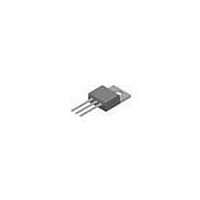
MC7800, MC7800A, NCV7805 PACKAGE DIMENSIONS TO-220, SINGLE GAUGE SUFFIX CASE 221AB-01 ISSUE O NOTES: 1. DIMENSIONING AND TOLERANCING PER ANSI Y14.5M, ...
Page 31
MC7800, MC7800A, NCV7805 OPTIONAL K A CHAMFER 0.010 (0.254 10.66 0.42 *For additional information on our Pb-Free strategy and soldering details, please download the ON Semiconductor ...
Page 32
0.13 (0.005) *For additional information on our Pb-Free strategy and soldering details, please download the ON Semiconductor Soldering and Mounting Techniques Reference Manual, SOLDERRM/D. ...