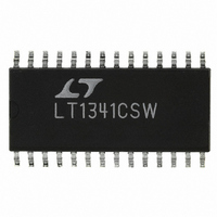
LT1341CSW Linear Technology, LT1341CSW Datasheet - Page 3

LT1341CSW
Manufacturer Part Number
LT1341CSW
Description
IC TXRX 5V RS232 W/SHTDWN 28SOIC
Manufacturer
Linear Technology
Type
Transceiverr
Datasheet
1.LT1341CSW.pdf
(8 pages)
Specifications of LT1341CSW
Number Of Drivers/receivers
3/5
Protocol
RS232
Voltage - Supply
4.5 V ~ 5.5 V
Mounting Type
Surface Mount
Package / Case
28-SOIC (7.5mm Width)
Lead Free Status / RoHS Status
Contains lead / RoHS non-compliant
Other names
LT1341CS
Available stocks
Company
Part Number
Manufacturer
Quantity
Price
Company:
Part Number:
LT1341CSW
Manufacturer:
NXP
Quantity:
3 171
Part Number:
LT1341CSW#PBF
Manufacturer:
LINEAR/凌特
Quantity:
20 000
Part Number:
LT1341CSW#TRPBF
Manufacturer:
LINEAR/凌特
Quantity:
20 000
PARAMETER
Any Driver
Output Voltage Swing
Logic Input Voltage Level
Logic Input Current
Output Short-Circuit Current
Output Leakage Current
Data Rate (Note 7)
Slew Rate
Propagation Delay
Any Receiver
Input Voltage Thresholds
Hysteresis
Input Resistance
Output Leakage Current
Receivers 1 Through 4
Output Voltage
Output Short-Circuit Current
Propagation Delay
Receiver 5 (Low-I
Output Voltage
Output Short-Circuit Current
Propagation Delay
The
temperature range (0 C T
Note 1: Absolute Maximum Ratings are those values beyond which the life
of the device may be impaired.
Note 2: Testing done at V
Note 3: Supply current is measured as the average over several charge
pump cycles. C
all driver inputs tied high.
Note 4: Supply current and leakage measurements in shutdown are
performed with V
disable are performed with V
ELECTRICAL C
denotes specifications which apply over the full operating
+
= C
ON/OFF
Q
RX)
–
= 0.1 F, C1 = C2 = 0.2 F. All outputs are open with
CC
0.1V. Supply current measurements using driver
A
= 5V and V
DRIVER DISABLE
HARA TERISTICS
70 C for commercial grade).
ON/OFF
C
CONDITIONS
Load = 3k to GND
Input Low Level (V
Input High Level (V
0.8V V
V
Shutdown V
R
R
R
R
Output Transition t
Output Transition t
Input Low Threshold (V
Input High Threshold (V
Shutdown (Note 4) 0 V
Output Low, I
Output High, I
Sinking Current, V
Sourcing Current, V
Output Transition t
Output Transition t
Output Low, I
Output High, I
Sinking Current, V
Sourcing Current, V
Output Transition t
Output Transition t
OUT
L
L
L
L
3V.
= 3k, C
= 3k, C
= 3k, C
= 3k, C
= 3V.
= 0V
IN
L
L
L
L
= 2500pF
= 1000pF
= 51pF
= 2500pF
OUT
2V
OUT
OUT
OUT
OUT
= 30V (Note 4)
= – 1.6mA
= – 500 A
= 160 A (V
= 160 A (V
OUT
OUT
HL
LH
HL
LH
HL
LH
OUT
OUT
OUT
OUT
High to Low (Note 5)
Low to High
High to Low (Note 6)
Low to High
High to Low (Note 6)
Low to High
= V
= V
= High)
= Low)
OUT
OUT
= 0V
= 0V
(Note 2)
OUT
CC
CC
= High)
= Low)
CC
CC
V
= 5V)
= 5V)
CC
Note 5: For driver delay measurements, R
points are set between the driver’s input logic threshold and the output
transition to the zero crossing (t
Note 6: For receiver delay measurements, C
set between the receiver’s input logic threshold and the output transition
to standard TTL/CMOS logic threshold (t
to 0.8V).
Note 7: Data rate operation guaranteed by slew rate, short-circuit current
and propagation delay tests.
Positive
Negative
HL
= 1.4V to 0V and t
MIN
120
250
0.8
0.1
3.5
3.5
10
5
2
4
3
2
9
HL
L
= 3k and C
L
= 1.3V to 2.4V and t
= 51pF. Trigger points are
– 6.5
TYP
– 20
250
350
1.4
1.4
0.6
0.5
1.3
1.7
0.4
0.2
4.2
0.2
4.2
– 4
10
15
5
5
1
1
1
7.3
17
6
20
4
LH
L
= 51pF. Trigger
= 1.4V to 0V).
MAX
– 10
100
600
600
– 5
0.8
1.3
1.3
2.4
1.0
0.4
0.4
– 2
20
30
10
7
3
3
LT1341
LH
= 1.7V
UNITS
kBaud
kBaud
3
V/ s
V/ s
mA
mA
mA
mA
mA
k
ns
ns
V
V
V
V
A
A
V
V
V
A
V
V
V
V
s
s
s
s


