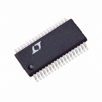
LTC2846IG#PBF Linear Technology, LTC2846IG#PBF Datasheet - Page 7

LTC2846IG#PBF
Manufacturer Part Number
LTC2846IG#PBF
Description
IC TXRX 3.3V MULTIPROTCOL 36SSOP
Manufacturer
Linear Technology
Type
Transceiverr
Datasheet
1.LTC2846CGPBF.pdf
(24 pages)
Specifications of LTC2846IG#PBF
Number Of Drivers/receivers
3/3
Protocol
Multiprotocol
Voltage - Supply
3.3V
Mounting Type
Surface Mount
Package / Case
36-SSOP
Interface Circuit Standard 1
RS-232
Number Of Receivers
3
Number Of Transmitters
3
Number Of Transceivers
1
Single Supply Voltage (typ)
3.3V
Single Supply Voltage (min)
3V
Single Supply Voltage (max)
3.6V
Dual Supply Voltage (typ)
Not RequiredV
Dual Supply Voltage (min)
Not RequiredV
Dual Supply Voltage (max)
Not RequiredV
Supply Current
170mA
Power Supply Requirement
Single
Operating Temp Range
-40C to 85C
Operating Temperature Classification
Industrial
Mounting
Surface Mount
Pin Count
36
Package Type
SSOP
Lead Free Status / RoHS Status
Lead free / RoHS Compliant
Available stocks
Company
Part Number
Manufacturer
Quantity
Price
PI FU CTIO S
NC (Pin 1): No Connect.
PGND (Pin 2): Boost Switching Regulator Power Ground.
Tie PGND to SGND.
V
switching regulator. 3V V
capacitor to ground.
SHDN (Pin 4): Boost Switching Regulator Shutdown Pin.
Tie to 2.4V or more to enable regulator. Ground to shut
down.
C1
1 F capacitor between C1
C1
1 F capacitor between C1
V
V.28. Connect a 1 F capacitor to ground.
V
ceiver. 4.75V V
ing regulator.
D1 (Pin 9): TTL Level Driver 1 Input.
D2 (Pin 10): TTL Level Driver 2 Input.
D3 (Pin 11): TTL Level Driver 3 Input.
R1 (Pin 12): CMOS Level Receiver 1 Output with Pull-Up
to V
R2 (Pin 13): CMOS Level Receiver 2 Output with Pull-Up
to V
R3 (Pin 14): CMOS Level Receiver 3 Output with Pull-Up
to V
M0 (Pin 15): TTL Level Mode Select Input 0 with Pull-Up
to V
M1 (Pin 16): TTL Level Mode Select Input 1 with Pull-Up
to V
V
3V V
IN
DD
CC
IN
–
+
U
(Pin 17): Input Supply Pin. Input supply to transceiver.
IN
IN
IN
IN
IN
(Pin 3): Input Supply Pin. Input supply to boost
(Pin 5): Capacitor C1 Negative Terminal. Connect a
(Pin 6): Capacitor C1 Positive Terminal. Connect a
(Pin 8): Input Supply Pin. Input supply to trans-
(Pin 7): Generated Positive Supply Voltage for
. See Table 1.
. See Table 1.
when Three-Stated.
when Three-Stated.
when Three-Stated.
IN
U
3.6V. Connect to Pin 3.
CC
U
5.25V. Connect to output of switch-
+
+
IN
and C1
and C1
3.6V. Bypass with a 10 F
–
–
.
.
M2 (Pin 18): TTL Level Mode Select Input 2 with Pull-Up
to V
DCE/DTE (Pin 19): TTL Level Mode Select Input with
Pull-Up to V
R3 B (Pin 20): Receiver 3 Noninverting Input.
R3 A (Pin 21): Receiver 3 Inverting Input.
R2 B (Pin 22): Receiver 2 Noninverting Input.
R2 A (Pin 23): Receiver 2 Inverting Input.
D3/R1 B (Pin 24): Receiver 1 Noninverting Input and
Driver 3 Noninverting Output.
D3/R1 A (Pin 25): Receiver 1 Inverting Input and Driver 3
Inverting Output.
D2 B (Pin 26): Driver 2 Noninverting Output.
D2 A (Pin 27): Driver 2 Inverting Output.
D1 B (Pin 28): Driver 1 Noninverting Output.
D1 A (Pin 29): Driver 1 Inverting Output.
GND (Pin 30): Transceiver Ground.
V
a 3.3 F capacitor to GND.
C2
1 F capacitor between C2
C2
1 F capacitor between C2
SGND (Pin 34): Boost Switching Regulator Signal Ground.
Tie PGND to SGND.
FB (Pin 35): Boost Switching Regulator Feedback Pin.
Reference voltage is 1.255V. Connect resistive divider tap
here. Minimize trace area at FB.
SW (Pin 36): Boost Switching Regulator Switch Pin.
Connect inductor/diode here. Minimize trace area at this
pin to reduce EMI.
EE
–
+
(Pin 31): Generated Negative Supply Voltage. Connect
IN
(Pin 32): Capacitor C2 Negative Terminal. Connect a
(Pin 33): Capacitor C2 Positive Terminal. Connect a
. See Table 1.
IN
. See Table 1.
+
+
and C2
and C2
–
–
.
.
LTC2846
sn2846 2846fs
7


