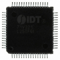
IDT82V1054APF IDT, Integrated Device Technology Inc, IDT82V1054APF Datasheet - Page 22

IDT82V1054APF
Manufacturer Part Number
IDT82V1054APF
Description
IC PCM CODEC 4CH MPI 3.3V 64TQFP
Manufacturer
IDT, Integrated Device Technology Inc
Type
Line Interface Units (LIUs)r
Datasheet
1.IDT82V1054APF8.pdf
(42 pages)
Specifications of IDT82V1054APF
Voltage - Supply
3.135 V ~ 3.465 V
Mounting Type
Surface Mount
Package / Case
64-TQFP, 64-VQFP
Lead Free Status / RoHS Status
Contains lead / RoHS non-compliant
Number Of Drivers/receivers
-
Protocol
-
Other names
82V1054APF
Available stocks
Company
Part Number
Manufacturer
Quantity
Price
Company:
Part Number:
IDT82V1054APF
Manufacturer:
IDT, Integrated Device Technology Inc
Quantity:
10 000
Company:
Part Number:
IDT82V1054APF8
Manufacturer:
IDT, Integrated Device Technology Inc
Quantity:
10 000
Company:
Part Number:
IDT82V1054APFG
Manufacturer:
IDT, Integrated Device Technology Inc
Quantity:
10 000
Company:
Part Number:
IDT82V1054APFG8
Manufacturer:
IDT, Integrated Device Technology Inc
Quantity:
10 000
IDT82V1054A QUAD PROGRAMMABLE PCM CODEC WITH MPI INTERFACE
3.4.2
For the global and local registers described below, it should be noted that:
1. R/W = 0, Read command. R/W = 1, Write command.
2. The reserved bit(s) in the registers must be filled in ‘0’ in write operation and be ignored in read operation.
GREG1: No Operation, Write (A0H); Version Number, Read (20H)
GREG2: Interrupt Clear, Write Only (A1H)
GREG3: Software Reset, Write Only (A2H)
GREG4: Hardware Reset, Write Only (A3)
GREG5: Chopper Clock Selection, Read/Write (24H/A4H)
GLOBAL REGISTERS LIST
By applying a read operation (20H) to this register, users can read out the version number of the IDT82V1054A. The default value is 01H.
To write to this register (no operation), a data byte of FFH must follow the write command (A0H) to ensure proper operation.
All interrupts on SLIC I/O will be cleared by applying a write operation to this register. Note that a data byte of FFH must follow the write
command (A1H) to ensure proper operation.
A write operation to this register resets all local registers, but does not reset global registers and the Coe-RAM. Note that when writing to
this register, a data byte of FFH must follow the write command (A2H) to ensure proper operation.
A write operation to this register is equivalent to setting the RESET pin to logic low (Refer to
for details). Note that when applying this write command, a data byte of FFH must follow to ensure proper operation.
This register is used to select the frequency of the CHclk2 and CHclk1 output signals.
CHclk2[1:0] = 00:
CHclk2[1:0] = 01:
CHclk2[1:0] = 10:
CHclk2[1:0] = 11:
CHclk1[3:0] = 0000:
CHclk1[3:0] = 0001:
CHclk1[3:0] = 0010:
CHclk1[3:0] = 0011:
CHclk1[3:0] = 0100:
CHclk1[3:0] = 0101:
CHclk1[3:0] = 0110:
CHclk1[3:0] = 0111:
CHclk1[3:0] = 1000:
Command
Command
Command
Command
Command
I/O data
R/W
R/W
b7
b7
b7
b7
b7
1
1
1
Reserved
chclk2 outputs a digital signal with the frequency of 256 kHz;
chclk2 outputs a digital signal with the frequency of 16384 kHz;
chclk1 outputs a digital signal with the frequency of 1000/2 Hz;
chclk1 outputs a digital signal with the frequency of 1000/4 Hz;
chclk1 outputs a digital signal with the frequency of 1000/8 Hz;
chclk1 outputs a digital signal with the frequency of 1000/10 Hz;
chclk1 outputs a digital signal with the frequency of 1000/12 Hz;
chclk1 outputs a digital signal with the frequency of 1000/16 Hz;
the output of chclk2 is set to high permanently (default);
chclk2 outputs a digital signal with the frequency of 512 kHz;
the output of chclk1 is set to high permanently (default);
chclk1 outputs a digital signal with the frequency of 1000/6 Hz;
chclk1 outputs a digital signal with the frequency of 1000/14 Hz;
b6
b6
b6
b6
b6
0
0
0
0
0
Chclk2[1]
b5
b5
b5
b5
b5
1
1
1
1
1
Chclk2[0]
22
b4
b4
b4
b4
b4
0
0
0
0
0
Chclk1[3]
b3
b3
b3
b3
b3
0
0
0
0
0
Chclk1[2]
b2
b2
b2
b2
b2
0
0
0
0
1
“3.3 Default State After Reset” on page 19
Chclk1[1]
b1
b1
b1
b1
b1
INDUSTRIAL TEMPERATURE
0
0
1
1
0
Chclk1[0]
b0
b0
b0
b0
b0
0
1
0
1
0


