JM38510/10306BIA National Semiconductor, JM38510/10306BIA Datasheet
JM38510/10306BIA
Specifications of JM38510/10306BIA


Related parts for JM38510/10306BIA


JM38510/10306BIA Summary of contents
Page 1
... LM119 much more versatile than older devices such as the LM711. Ordering Information NS Part Number JAN Part Number JL119BIA JM38510/10306BIA JL119BCA JM38510/10306BCA Connection Diagrams Dual-In-Line Package Top View See NS Package Number J14A © ...
Page 2
Schematic Diagram *Do not operate the LM119 with more than 16V between GND and V www.national.com + 2 201481 Version 2 Revision 3 Print Date/Time: 2010/09/30 23:38:32 20148101 ...
Page 3
Absolute Maximum Ratings Total Supply Voltage Output to Negative Supply Voltage Ground to Negative Supply Voltage Ground to Positive Supply Voltage Differential Input Voltage Input Voltage (Note 3) Power Dissipation (Note 2) Output Short Circuit Duration Storage Temperature Range Operating ...
Page 4
Electrical Characteristics DC Parameters Symbol Parameter V Input Offset Voltage IO I Input Offset Current IO +I Power Supply Current CC -I Power Supply Current CC ±I Input Bias Current IB CMRR Common Mode Rejection V Low Level Output Voltage ...
Page 5
AC Parameters The following conditions apply to all the following parameters, unless otherwise specified. AC: ±15V 50pF L Symbol Parameter tR Response Time (Collector LHC Output) tR Response Time (Collector HLC Output) DC Drift Parameters Delta calculations performed ...
Page 6
Typical Performance Characteristics Input Currents Transfer Function Response Time for Various Input Overdrives www.national.com 20148110 20148112 20148114 6 201481 Version 2 Revision 3 Print Date/Time: 2010/09/30 23:38:32 Common Mode Limits 20148111 Response Time for Various Input Overdrives 20148113 Input Characteristics ...
Page 7
Response Time for Various Input Overdrives 20148116 Output Saturation Voltage 20148118 Supply Current 20148120 201481 Version 2 Revision 3 Response Time for Various Input Overdrives Supply Current Output Limiting Characteristics 7 Print Date/Time: 2010/09/30 23:38:32 20148117 20148119 20148121 www.national.com ...
Page 8
Typical Applications Relay Driver Note 6: Pin numbers are for metal can package. www.national.com (Note Pin numbers are for metal can package. 20148105 for V OUT for V OUT 8 201481 Version 2 Revision ...
Page 9
Revision History Section Date Released Revision Section 7/0105 A 09/24/2010 B Obsolete Data Sheet 201481 Version 2 Revision 3 New release to corporate format 9 Print Date/Time: 2010/09/30 23:38:32 Changes 1 MDS datasheet converted into one corporate data sheet format ...
Page 10
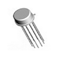
Physical Dimensions www.national.com inches (millimeters) unless otherwise noted Metal Can Package (H) NS Package Number H10C Cavity Dual-In-Line Package (J) NS Package Number J14A 10 201481 Version 2 Revision 3 Print Date/Time: 2010/09/30 23:38:32 ...
Page 11
Notes 11 201481 Version 2 Revision 3 Print Date/Time: 2010/09/30 23:38:32 www.national.com ...
Page 12
... For more National Semiconductor product information and proven design tools, visit the following Web sites at: www.national.com Products Amplifiers www.national.com/amplifiers Audio www.national.com/audio Clock and Timing www.national.com/timing Data Converters www.national.com/adc Interface www.national.com/interface LVDS www.national.com/lvds Power Management www.national.com/power Switching Regulators www.national.com/switchers LDOs www.national.com/ldo LED Lighting www ...