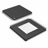
DS26303LN-75+ Maxim Integrated Products, DS26303LN-75+ Datasheet - Page 45

DS26303LN-75+
Manufacturer Part Number
DS26303LN-75+
Description
IC LIU E1/T1/J1 3.3V 144-ELQFP
Manufacturer
Maxim Integrated Products
Type
Line Interface Units (LIUs)r
Datasheet
1.DS26303L-120.pdf
(101 pages)
Specifications of DS26303LN-75+
Number Of Drivers/receivers
8/8
Protocol
T1/E1/J1
Voltage - Supply
3.135 V ~ 3.465 V
Mounting Type
Surface Mount
Package / Case
144-LQFP Exposed Pad, 144-eLQFP, 144-HLQFP
Lead Free Status / RoHS Status
Lead free / RoHS Compliant
- Current page: 45 of 101
- Download datasheet (2Mb)
Register Name:
Register Description:
Register Address:
Bit #
Name
Default
Bits 7 to 5: PLL Clock Select (PCLKS[2:0]). These bits determine the RCLK that is to be used as the input to the
PLL. If an LOS is detected for the channel that RCLK is recovered from, the PLL switches to MCLK until the LOS is
cleared. When the LOS is cleared, the selected RCLK is used again. See
Table 5-15. PLL Clock Select
Bit 4: T1/E1 Clock Select (TECLKS). When this bit is set the T1/E1 clock output is 2.048MHz. When this bit is
reset the T1/E1 clock rate is 1.544MHz.
Bits 3 to 0: Clock A Select (CLKA[3:0]). These bits select the output frequency for CLKA pin. See
available frequencies.
Table 5-16. Clock A Select
PCLKS[2:0]
CLKA[3:0]
000
001
010
011
100
101
110
111
0000
0001
0010
0011
0100
0101
0110
0111
1000
1001
1010
1011
1100
1101
1110
1111
PCLKS2
7
0
MC.PCLKI = 1
PCLKS1
PLL CLOCK
SELECTED
RCLK1
RCLK2
RCLK3
RCLK4
RCLK5
RCLK6
RCLK7
RCLK8
6
0
MCLK (Hz)
16.384M
12.352M
12.288M
2.048M
4.096M
8.192M
1.544M
3.088M
6.176M
1.536M
3.072M
6.144M
128k
256k
CCR
Clock Control Register
15h
32k
64k
PCLKS0
5
0
TECLKS
DS26303: 3.3V, T1/E1/J1, Short-Haul, Octal Line Interface Unit
45 of 101
4
0
CLKA3
3
0
Table 5-15
CLKA2
2
0
for RCLK selection.
CLKA1
1
0
Table 5-16
CLKA0
0
0
for
Related parts for DS26303LN-75+
Image
Part Number
Description
Manufacturer
Datasheet
Request
R

Part Number:
Description:
IC LIU E1/T1/J1 3.3V 144-ELQFP
Manufacturer:
Maxim Integrated Products
Datasheet:

Part Number:
Description:
IC LIU E1/T1/J1 3.3V 144-ELQFP
Manufacturer:
Maxim Integrated Products
Datasheet:

Part Number:
Description:
Buffers & Line Drivers 3.3V E1/T1/J1 Short Haul Octal LIU
Manufacturer:
Maxim Integrated Products

Part Number:
Description:
Buffers & Line Drivers 3.3V E1/T1/J1 Short Haul Octal LIU
Manufacturer:
Maxim Integrated Products

Part Number:
Description:
Buffers & Line Drivers 3.3V E1/T1/J1 Short Haul Octal LIU
Manufacturer:
Maxim Integrated Products

Part Number:
Description:
Buffers & Line Drivers 3.3V E1/T1/J1 Short Haul Octal LIU
Manufacturer:
Maxim Integrated Products

Part Number:
Description:
Buffers & Line Drivers 3.3V E1/T1/J1 Short Haul Octal LIU
Manufacturer:
Maxim Integrated Products

Part Number:
Description:
Buffers & Line Drivers 3.3V E1/T1/J1 Short Haul Octal LIU
Manufacturer:
Maxim Integrated Products

Part Number:
Description:
Buffers & Line Drivers 3.3V E1/T1/J1 Short Haul Octal LIU
Manufacturer:
Maxim Integrated Products

Part Number:
Description:
TYPE DS FUSED DISCONNECT SWITCH 60A 3P
Manufacturer:
EATON CUTLER HAMMER

Part Number:
Description:
MAX7528KCWPMaxim Integrated Products [CMOS Dual 8-Bit Buffered Multiplying DACs]
Manufacturer:
Maxim Integrated Products
Datasheet:

Part Number:
Description:
Single +5V, fully integrated, 1.25Gbps laser diode driver.
Manufacturer:
Maxim Integrated Products
Datasheet:

Part Number:
Description:
Single +5V, fully integrated, 155Mbps laser diode driver.
Manufacturer:
Maxim Integrated Products
Datasheet:

Part Number:
Description:
VRD11/VRD10, K8 Rev F 2/3/4-Phase PWM Controllers with Integrated Dual MOSFET Drivers
Manufacturer:
Maxim Integrated Products
Datasheet:


