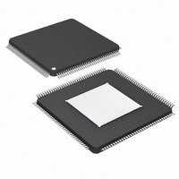
DS26303LN-75+ Maxim Integrated Products, DS26303LN-75+ Datasheet - Page 64

DS26303LN-75+
Manufacturer Part Number
DS26303LN-75+
Description
IC LIU E1/T1/J1 3.3V 144-ELQFP
Manufacturer
Maxim Integrated Products
Type
Line Interface Units (LIUs)r
Datasheet
1.DS26303L-120.pdf
(101 pages)
Specifications of DS26303LN-75+
Number Of Drivers/receivers
8/8
Protocol
T1/E1/J1
Voltage - Supply
3.135 V ~ 3.465 V
Mounting Type
Surface Mount
Package / Case
144-LQFP Exposed Pad, 144-eLQFP, 144-HLQFP
Lead Free Status / RoHS Status
Lead free / RoHS Compliant
- Current page: 64 of 101
- Download datasheet (2Mb)
6.6 Jitter Attenuator
The DS26303 contains an on-board jitter attenuator that can be set to a depth of either 32 or 128 bits by the JADS
bit in register
bit mode is used in applications where large excursions of wander are expected. The 32-bit mode is used in delay-
sensitive applications. The characteristics of the attenuation are shown in
placed in either the receive path or the transmit path or none by appropriately setting the JAPS and the JAE bits in
register GC. These selections can be changed on an individual LIU basis by settings in the
For the jitter attenuator to properly operate, a 2.048MHz or multiple thereof, or 1.544MHz clock or multiple thereof
must be applied at MCLK. ITU-T specification G.703 requires an accuracy of ±50ppm for both T1 and E1
applications. TR62411 and ANSI specs require an accuracy of ±32ppm for T1 interfaces. On-board circuitry adjusts
either the recovered clock from the clock/data recovery block or the clock applied at the TCLKn pin to create a
smooth jitter-free clock, which is used to clock data out of the jitter attenuator FIFO. It is acceptable to provide a
gapped/bursty clock at the TCLKn pin if the jitter attenuator is placed on the transmit side. If the incoming jitter
exceeds either 120UI
internal nominal 32.768MHz (E1) or 24.704MHz (T1) clock by either 15 or 17 instead of the normal 16 to keep the
buffer from overflowing. When the device divides by either 15 or 17, it also sets the jitter attenuator limit trip
(IJAFLTn) bits in the
Figure 6-7. Jitter Attenuation
GC.
It can also be controlled on an individual LIU basis by settings in the
-20dB
-40dB
-60dB
IJAFLT
P-P
0dB
(buffer depth is 128 bits) or 28UI
1
register described.
10
E1
Prohibited
TBR12
Area
T1
DS26303: 3.3V, T1/E1/J1, Short-Haul, Octal Line Interface Unit
64 of 101
100
FREQUENCY (Hz)
P-P
(buffer depth is 32 bits), then the DS26303 divides the
1K
Prohibited Area
ITU G.7XX
TR 62411 (Dec. 90)
Figure
Prohibited Area
10K
6-7. The jitter attenuator can be
IJAFDS
IJAPS
100K
register. The 128-
and IJAE.
6 6 6 6 6
Related parts for DS26303LN-75+
Image
Part Number
Description
Manufacturer
Datasheet
Request
R

Part Number:
Description:
IC LIU E1/T1/J1 3.3V 144-ELQFP
Manufacturer:
Maxim Integrated Products
Datasheet:

Part Number:
Description:
IC LIU E1/T1/J1 3.3V 144-ELQFP
Manufacturer:
Maxim Integrated Products
Datasheet:

Part Number:
Description:
Buffers & Line Drivers 3.3V E1/T1/J1 Short Haul Octal LIU
Manufacturer:
Maxim Integrated Products

Part Number:
Description:
Buffers & Line Drivers 3.3V E1/T1/J1 Short Haul Octal LIU
Manufacturer:
Maxim Integrated Products

Part Number:
Description:
Buffers & Line Drivers 3.3V E1/T1/J1 Short Haul Octal LIU
Manufacturer:
Maxim Integrated Products

Part Number:
Description:
Buffers & Line Drivers 3.3V E1/T1/J1 Short Haul Octal LIU
Manufacturer:
Maxim Integrated Products

Part Number:
Description:
Buffers & Line Drivers 3.3V E1/T1/J1 Short Haul Octal LIU
Manufacturer:
Maxim Integrated Products

Part Number:
Description:
Buffers & Line Drivers 3.3V E1/T1/J1 Short Haul Octal LIU
Manufacturer:
Maxim Integrated Products

Part Number:
Description:
Buffers & Line Drivers 3.3V E1/T1/J1 Short Haul Octal LIU
Manufacturer:
Maxim Integrated Products

Part Number:
Description:
TYPE DS FUSED DISCONNECT SWITCH 60A 3P
Manufacturer:
EATON CUTLER HAMMER

Part Number:
Description:
MAX7528KCWPMaxim Integrated Products [CMOS Dual 8-Bit Buffered Multiplying DACs]
Manufacturer:
Maxim Integrated Products
Datasheet:

Part Number:
Description:
Single +5V, fully integrated, 1.25Gbps laser diode driver.
Manufacturer:
Maxim Integrated Products
Datasheet:

Part Number:
Description:
Single +5V, fully integrated, 155Mbps laser diode driver.
Manufacturer:
Maxim Integrated Products
Datasheet:

Part Number:
Description:
VRD11/VRD10, K8 Rev F 2/3/4-Phase PWM Controllers with Integrated Dual MOSFET Drivers
Manufacturer:
Maxim Integrated Products
Datasheet:


