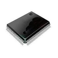
ST92F120V1Q7 STMicroelectronics, ST92F120V1Q7 Datasheet - Page 143

ST92F120V1Q7
Manufacturer Part Number
ST92F120V1Q7
Description
Microcontrollers (MCU) Flash 128K SPI/I2C
Manufacturer
STMicroelectronics
Datasheet
1.ST92F120V9Q7.pdf
(325 pages)
Specifications of ST92F120V1Q7
Data Bus Width
8 bit, 16 bit
Program Memory Type
Flash
Program Memory Size
128 KB
Data Ram Size
4 KB
Interface Type
I2C, SPI
Maximum Clock Frequency
24 MHz
Number Of Programmable I/os
77
Number Of Timers
5
Maximum Operating Temperature
+ 105 C
Mounting Style
SMD/SMT
Package / Case
PQFP-100
Minimum Operating Temperature
- 40 C
On-chip Adc
8 bit, 16 Channel
Lead Free Status / Rohs Status
No
Available stocks
Company
Part Number
Manufacturer
Quantity
Price
Company:
Part Number:
ST92F120V1Q7
Manufacturer:
ST
Quantity:
6 765
Part Number:
ST92F120V1Q7
Manufacturer:
ST
Quantity:
20 000
Part Number:
ST92F120V1Q7C
Manufacturer:
ST
Quantity:
20 000
Company:
Part Number:
ST92F120V1Q7DTR
Manufacturer:
MAXIM
Quantity:
2 854
- Current page: 143 of 325
- Download datasheet (3Mb)
EXTENDED FUNCTION TIMER (Cont’d)
10.3.3.5 Forced Compare Mode
In this section i may represent 1 or 2.
The following bits of the CR1 register are used:
When the FOLV i bit is set, the OLVL i bit is copied
to the OCMP i pin. The OLVL i bit has to be toggled
in order to toggle the OCMP i pin when it is enabled
(OC i E bit=1).
The OCF i bit is not set, and thus no interrupt re-
quest is generated.
10.3.3.6 One Pulse Mode
One Pulse mode enables the generation of a
pulse when an external event occurs. This mode is
selected via the OPM bit in the CR2 register.
The one pulse mode uses the Input Capture1
function and the Output Compare1 function.
Procedure
To use one pulse mode, select the following in the
the CR1 register:
– Using the OLVL1 bit, select the level to be ap-
– Using the OLVL2 bit, select the level to be ap-
– Select the edge of the active transition on the
And select the following in the CR2 register:
– Set the OC1E bit, the OCMP1 pin is then dedi-
– Set the OPM bit.
– Select the timer clock CC[1:0] (see
Figure 81. One Pulse Mode Timing
plied to the OCMP1 pin after the pulse.
plied to the OCMP1 pin during the pulse.
ICAP1 pin with the IEDG1 bit .
cated to the Output Compare 1 function.
COUNTER
Note: IEDG1=1, OC1R=2ED0h, OLVL1=0, OLVL2=1
OCMP1
ICAP1
FOLV2 FOLV1 OLVL2
....
FFFC FFFD FFFE
Table
OLVL2
OLVL1
28).
Load the OC1R register with the value corre-
sponding to the length of the pulse (see the formu-
la in
Then, on a valid event on the ICAP1 pin, the coun-
ter is initialized to FFFCh and OLVL2 bit is loaded
on the OCMP1 pin. When the value of the counter
is equal to the value of the contents of the OC1R
register, the OLVL1 bit is output on the OCMP1
pin, (See
Note: The OCF1 bit cannot be set by hardware in
one pulse mode but the OCF2 bit can generate an
Output Compare interrupt.
The ICF1 bit is set when an active edge occurs
and can generate an interrupt if the ICIE bit is set.
When the Pulse Width Modulation (PWM) and
One Pulse Mode (OPM) bits are both set, the
PWM mode is the only active one.
compare1
2ED0 2ED1 2ED2
Section
EXTENDED FUNCTION TIMER (EFT)
event occurs
on ICAP1
Counter
= OC1R
When
Figure
When
10.3.3.7).
OLVL1
81).
2ED3
One pulse mode cycle
OCMP1 = OLVL2
FFFC FFFD
OCMP1 = OLVL1
Counter is
initialized
to FFFCh
OLVL2
143/324
9
Related parts for ST92F120V1Q7
Image
Part Number
Description
Manufacturer
Datasheet
Request
R

Part Number:
Description:
8/16-bit Flash Mcu Family With Ram, Eeprom And J1850 Blpd
Manufacturer:
STMicroelectronics
Datasheet:

Part Number:
Description:
STMicroelectronics [RIPPLE-CARRY BINARY COUNTER/DIVIDERS]
Manufacturer:
STMicroelectronics
Datasheet:

Part Number:
Description:
STMicroelectronics [LIQUID-CRYSTAL DISPLAY DRIVERS]
Manufacturer:
STMicroelectronics
Datasheet:

Part Number:
Description:
BOARD EVAL FOR MEMS SENSORS
Manufacturer:
STMicroelectronics
Datasheet:

Part Number:
Description:
NPN TRANSISTOR POWER MODULE
Manufacturer:
STMicroelectronics
Datasheet:

Part Number:
Description:
TURBOSWITCH ULTRA-FAST HIGH VOLTAGE DIODE
Manufacturer:
STMicroelectronics
Datasheet:

Part Number:
Description:
Manufacturer:
STMicroelectronics
Datasheet:

Part Number:
Description:
DIODE / SCR MODULE
Manufacturer:
STMicroelectronics
Datasheet:

Part Number:
Description:
DIODE / SCR MODULE
Manufacturer:
STMicroelectronics
Datasheet:

Part Number:
Description:
Search -----> STE16N100
Manufacturer:
STMicroelectronics
Datasheet:

Part Number:
Description:
Search ---> STE53NA50
Manufacturer:
STMicroelectronics
Datasheet:

Part Number:
Description:
NPN Transistor Power Module
Manufacturer:
STMicroelectronics
Datasheet:


