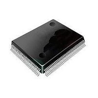
ST92F120V1Q7 STMicroelectronics, ST92F120V1Q7 Datasheet - Page 173

ST92F120V1Q7
Manufacturer Part Number
ST92F120V1Q7
Description
Microcontrollers (MCU) Flash 128K SPI/I2C
Manufacturer
STMicroelectronics
Datasheet
1.ST92F120V9Q7.pdf
(325 pages)
Specifications of ST92F120V1Q7
Data Bus Width
8 bit, 16 bit
Program Memory Type
Flash
Program Memory Size
128 KB
Data Ram Size
4 KB
Interface Type
I2C, SPI
Maximum Clock Frequency
24 MHz
Number Of Programmable I/os
77
Number Of Timers
5
Maximum Operating Temperature
+ 105 C
Mounting Style
SMD/SMT
Package / Case
PQFP-100
Minimum Operating Temperature
- 40 C
On-chip Adc
8 bit, 16 Channel
Lead Free Status / Rohs Status
No
Available stocks
Company
Part Number
Manufacturer
Quantity
Price
Company:
Part Number:
ST92F120V1Q7
Manufacturer:
ST
Quantity:
6 765
Part Number:
ST92F120V1Q7
Manufacturer:
ST
Quantity:
20 000
Part Number:
ST92F120V1Q7C
Manufacturer:
ST
Quantity:
20 000
Company:
Part Number:
ST92F120V1Q7DTR
Manufacturer:
MAXIM
Quantity:
2 854
- Current page: 173 of 325
- Download datasheet (3Mb)
MULTIFUNCTION TIMER (Cont’d)
OUTPUT A CONTROL REGISTER (OACR)
R252 - Read/Write
Register Page: 10
Reset value: 0000 0000
Bits 7:6 = C0E[0:1]: COMP0 action bits .
These bits are set and cleared by software. They
configure the action to be performed on the Tx-
OUTA pin when a successful compare of the
CMP0R register occurs. Refer to
list of actions that can be configured.
Bits 5:4 = C1E[0:1]: COMP1 action bits .
These bits are set and cleared by software. They
configure the action to be performed on the Tx-
OUTA pin when a successful compare of the
CMP1R register occurs. Refer to
list of actions that can be configured.
Bits 3:2 = OUE[0:1]: OVF/UNF action bits .
These bits are set and cleared by software. They
configure the action to be performed on the Tx-
OUTA pin when an Overflow or Underflow of the
U/D counter occurs. Refer to
actions that can be configured.
C0E0 C0E1 C1E0 C1E1 OUE0 OUE1 CEV 0P
7
Table 5
Table 5
Table 5
for the list of
0
for the
for the
Table 35. Output A Action Bits
Notes:
– xx stands for C0, C1 or OU.
– Whenever more than one event occurs simulta-
Bit 1 = CEV: On-Chip event on CMP0R .
This bit is set and cleared by software.
0: No action
1: A successful compare on CMP0R activates the
Bit 0 = OP: TxOUTA preset value .
This bit is set and cleared by software and by hard-
ware. The value of this bit is the preset value of the
TxOUTA pin. Reading this bit returns the current
state of the TxOUTA pin (useful when it is selected
in toggle mode).
xxE0
0
0
1
1
neously, Action bit 0 will be the result of ANDing
Action bit 0 of all simultaneous events and Action
bit 1 will be the result of ANDing Action bit 1 of all
simultaneous events.
on-chip event signal (a single pulse is generat-
ed)
xxE1
0
1
0
1
MULTIFUNCTION TIMER (MFT)
Action on TxOUTA pin when an xx
event occurs
Set
Toggle
Reset
NOP
173/324
9
Related parts for ST92F120V1Q7
Image
Part Number
Description
Manufacturer
Datasheet
Request
R

Part Number:
Description:
8/16-bit Flash Mcu Family With Ram, Eeprom And J1850 Blpd
Manufacturer:
STMicroelectronics
Datasheet:

Part Number:
Description:
STMicroelectronics [RIPPLE-CARRY BINARY COUNTER/DIVIDERS]
Manufacturer:
STMicroelectronics
Datasheet:

Part Number:
Description:
STMicroelectronics [LIQUID-CRYSTAL DISPLAY DRIVERS]
Manufacturer:
STMicroelectronics
Datasheet:

Part Number:
Description:
BOARD EVAL FOR MEMS SENSORS
Manufacturer:
STMicroelectronics
Datasheet:

Part Number:
Description:
NPN TRANSISTOR POWER MODULE
Manufacturer:
STMicroelectronics
Datasheet:

Part Number:
Description:
TURBOSWITCH ULTRA-FAST HIGH VOLTAGE DIODE
Manufacturer:
STMicroelectronics
Datasheet:

Part Number:
Description:
Manufacturer:
STMicroelectronics
Datasheet:

Part Number:
Description:
DIODE / SCR MODULE
Manufacturer:
STMicroelectronics
Datasheet:

Part Number:
Description:
DIODE / SCR MODULE
Manufacturer:
STMicroelectronics
Datasheet:

Part Number:
Description:
Search -----> STE16N100
Manufacturer:
STMicroelectronics
Datasheet:

Part Number:
Description:
Search ---> STE53NA50
Manufacturer:
STMicroelectronics
Datasheet:

Part Number:
Description:
NPN Transistor Power Module
Manufacturer:
STMicroelectronics
Datasheet:


