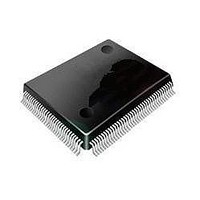
ST92F120V1Q7 STMicroelectronics, ST92F120V1Q7 Datasheet - Page 6

ST92F120V1Q7
Manufacturer Part Number
ST92F120V1Q7
Description
Microcontrollers (MCU) Flash 128K SPI/I2C
Manufacturer
STMicroelectronics
Datasheet
1.ST92F120V9Q7.pdf
(325 pages)
Specifications of ST92F120V1Q7
Data Bus Width
8 bit, 16 bit
Program Memory Type
Flash
Program Memory Size
128 KB
Data Ram Size
4 KB
Interface Type
I2C, SPI
Maximum Clock Frequency
24 MHz
Number Of Programmable I/os
77
Number Of Timers
5
Maximum Operating Temperature
+ 105 C
Mounting Style
SMD/SMT
Package / Case
PQFP-100
Minimum Operating Temperature
- 40 C
On-chip Adc
8 bit, 16 Channel
Lead Free Status / Rohs Status
No
Available stocks
Company
Part Number
Manufacturer
Quantity
Price
Company:
Part Number:
ST92F120V1Q7
Manufacturer:
ST
Quantity:
6 765
Part Number:
ST92F120V1Q7
Manufacturer:
ST
Quantity:
20 000
Part Number:
ST92F120V1Q7C
Manufacturer:
ST
Quantity:
20 000
Company:
Part Number:
ST92F120V1Q7DTR
Manufacturer:
MAXIM
Quantity:
2 854
- Current page: 6 of 325
- Download datasheet (3Mb)
ST92F120 - GENERAL DESCRIPTION
1.2 PIN DESCRIPTION
AS. Address Strobe (output, active low, 3-state).
Address Strobe is pulsed low once at the begin-
ning of each memory cycle. The rising edge of AS
indicates that address, Read/Write (RW), and
Data signals are valid for memory transfers.
DS. Data Strobe (output, active low, 3-state). Data
Strobe provides the timing for data movement to or
from Port 0 for each memory transfer. During a
write cycle, data out is valid at the leading edge of
DS. During a read cycle, Data In must be valid pri-
or to the trailing edge of DS. When the ST9 ac-
cesses on-chip memory, DS is held high during
the whole memory cycle.
RESET. Reset (input, active low). The ST9 is ini-
tialised by the Reset signal. With the deactivation
of RESET, program execution begins from the
Program memory location pointed to by the vector
contained in program memory locations 00h and
01h.
RW. Read/Write (output, 3-state). Read/Write de-
termines the direction of data transfer for external
memory transactions. RW is low when writing to
external memory, and high for all other transac-
tions.
OSCIN, OSCOUT. Oscillator (input and output).
These pins connect a parallel-resonant crystal, or
an external source to the on-chip clock oscillator
and buffer. OSCIN is the input of the oscillator in-
verter and internal clock generator; OSCOUT is
the output of the oscillator inverter.
HW0SW1. When connected to V
pull-up resistor, the software watchdog option is
selected. When connected to V
pull-down resistor, the hardware watchdog option
is selected.
VPWO. This pin is the output line of the J1850 pe-
ripheral (JBLPD). It is available only on some de-
vices. On devices without JBLPD peripheral, this
pin must not be connected.
P0[7:0], P1[2:0] or P1[7:0] (Input/Output, TTL or
CMOS compatible) . 16 lines providing the external
memory interface for addressing 2K or 64 K bytes
of external memory.
P0[7:0], P1[2:0], P2[7:0], P3[7:4], P4[7:4],
P5[7:0], P6[5:2,0], P7[7:0] I/O Port Lines (Input/
Output, TTL or CMOS compatible) . I/O lines
grouped into I/O ports of 8 bits, bit programmable
under software control as general purpose I/O or
as alternate functions.
6/324
9
SS
DD
through a 1K
through a 1K
P1[7:3], P3[3:1], P4[3:0], P6.1, P8[7:0], P9[7:0]
Additional I/O Port Lines available on PQFP100
versions only.
AV
er (common for A/D 0 and A/D 1).
AV
er (common for A/D 0 and A/D 1).
V
available. The pins are internally connected.
V
ble. The pins are internally connected.
V
poses. This pin is bonded and must be kept to 0 in
User mode.
V
ST92F124 and ST92F150).
1.2.1 Electromagnetic Compatibility (EMC)
To reduce the electromagnetic interference the fol-
lowing features have been implemented:
– A low power oscillator is included with a control-
– Four pairs of digital power supply pins (V
– Digital and analog power supplies are complete-
– Digital power supplies for internal logic and I/O
– Internal decoupling capacitance is located be-
Note: Each pair of digital V
externally connected by a 10 F chemical pulling
capacitor and a 100 nF ceramic chip capacitor.
1.2.2 I/O Port Alternate Functions
Each pin of the I/O ports of the ST92F120 may as-
sume software programmable Alternate Functions
as shown in
1.2.3 Termination of Unused Pins
The ST9 device is implemented using CMOS tech-
nology; therefore unused pins must be properly
terminated in order to avoid application reliability
problems. In fact, as shown in
ard input circuitry is based on the CMOS inverter
structure.
DD
SS
TEST
REG
led gain to reduce EMI and the power consump-
tion in Halt mode.
V
ly separated.
ports are separated internally.
tween V
DD
SS
SS
Digital Circuit Ground. Four pins are availa-
Main Power Supply Voltage. Four pins are
Analog V
Analog V
3V regulator output (on future versions, i.e.
) are located on each side of the package.
Power Supply Voltage for Flash test pur-
DD
Section
and V
SS
DD
of the Analog to Digital Convert-
of the Analog to Digital Convert-
SS
1.3.
.
DD
/V
Figure
SS
pins should be
2, the stand-
DD
,
Related parts for ST92F120V1Q7
Image
Part Number
Description
Manufacturer
Datasheet
Request
R

Part Number:
Description:
8/16-bit Flash Mcu Family With Ram, Eeprom And J1850 Blpd
Manufacturer:
STMicroelectronics
Datasheet:

Part Number:
Description:
STMicroelectronics [RIPPLE-CARRY BINARY COUNTER/DIVIDERS]
Manufacturer:
STMicroelectronics
Datasheet:

Part Number:
Description:
STMicroelectronics [LIQUID-CRYSTAL DISPLAY DRIVERS]
Manufacturer:
STMicroelectronics
Datasheet:

Part Number:
Description:
BOARD EVAL FOR MEMS SENSORS
Manufacturer:
STMicroelectronics
Datasheet:

Part Number:
Description:
NPN TRANSISTOR POWER MODULE
Manufacturer:
STMicroelectronics
Datasheet:

Part Number:
Description:
TURBOSWITCH ULTRA-FAST HIGH VOLTAGE DIODE
Manufacturer:
STMicroelectronics
Datasheet:

Part Number:
Description:
Manufacturer:
STMicroelectronics
Datasheet:

Part Number:
Description:
DIODE / SCR MODULE
Manufacturer:
STMicroelectronics
Datasheet:

Part Number:
Description:
DIODE / SCR MODULE
Manufacturer:
STMicroelectronics
Datasheet:

Part Number:
Description:
Search -----> STE16N100
Manufacturer:
STMicroelectronics
Datasheet:

Part Number:
Description:
Search ---> STE53NA50
Manufacturer:
STMicroelectronics
Datasheet:

Part Number:
Description:
NPN Transistor Power Module
Manufacturer:
STMicroelectronics
Datasheet:


