HMP8156ACNZ Intersil, HMP8156ACNZ Datasheet
HMP8156ACNZ
Specifications of HMP8156ACNZ
Available stocks


Related parts for HMP8156ACNZ

HMP8156ACNZ Summary of contents
Page 1
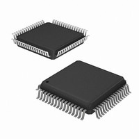
... MARKING (°C) PACKAGE HMP8154CN HMP8154C PQFP Q64.14x14 N HMP8156ACN HMP8156A PQFP Q64.14x14 CN HMP8156ACNZ HMP8156A PQFP (See Note) CNZ (Pb-free) HMP8154EVAL1 Daughter/Stand-Alone Card Evaluation Platform* HMP8156EVAL1 HMP8156EVAL2 Frame Grabber Evaluation Platform* *Described in the Applications Section NOTE: Intersil Pb-free plus anneal products employ special Pb-free material sets ...
Page 2
Functional Block Diagram P0 - P23 Y/Cb/Cr OPTIONAL 4:4:4 GAMMA (2:2:2 SIF) CORRECTION COLOR SPACE CONVERSION 4:2:2 TO 4:4:4 SAMPLE CONVERSION SA SCL HOST INTERFACE SDA RESET HSYNC VSYNC VIDEO BLANK TIMING CONTROL CLK CLK2 FIELD OVERLAY PROCESSING FLICKER 2X ...
Page 3
Functional Operation The HMP8154 and HMP8156A are fully integrated digital encoders. Either accepts digital video input data and generates four analog video output signals. The input data format is selectable and includes YCbCr, RGB, and overlay data. The outputs are ...
Page 4
PIN 4:2:2 NAME YCBCR P0 Cb0, Cr0 P1 Cb1, Cr1 P2 Cb2, Cr2 P3 Cb3, Cr3 P4 Cb4, Cr4 P5 Cb5, Cr5 P6 Cb6, Cr6 P7 Cb7, Cr7 P10 Y2 P11 Y3 P12 Y4 P13 ...
Page 5
When going from overlay to pixel data, mixing starts one pixel before the selection of the pixel color (OL2-OL0 = 000). The last pixel output of the overlay uses 87.5% overlay color plus 12.5% pixel color. The next output uses ...
Page 6
TABLE 5. PIXEL INPUT AND CONTROL SIGNAL I/O TIMING INPUT PORT SAMPLING INPUT FORMAT PIXEL DATA 8-Bit YCbCr Norm Every rising edge of CLK2 2X Rising edge of CLK2 when CLK is low. FF 16-Bit YCbCr, Norm Rising edge of ...
Page 7
CLK2 P8-P15 Cb 0 OL0-OL2, M1, M0 BLANK (INPUT) BLANK (OUTPUT) FIGURE 1. PIXEL AND OVERLAY INPUT TIMING - NORMAL 8-BIT YCBCR CLK2 CLK P8-P15 Cb 0 OL0-OL2, M1, M0 BLANK (INPUT) BLANK (OUTPUT) FIGURE 2. PIXEL AND OVERLAY INPUT ...
Page 8
CLK2 CLK P8-P15 Y 0 P0- OL0-OL2, PIXEL 0 M1, M0 BLANK (INPUT) BLANK (OUTPUT) FIGURE 3. PIXEL AND OVERLAY INPUT TIMING - NORMAL 16-BIT YCBCR CLK2 CLK RGB 0 P0-P15 OL0-OL2, PIXEL 0 M1, M0 BLANK (INPUT) ...
Page 9
YCbCr, 16-Bit RGB, 24-Bit RGB Formats with 2X Upscaling When 16-bit YCbCr, 16-bit RGB data, or 24-bit RGB format is selected and 2X upscaling is enabled, data is latched on the rising edge of CLK2 while CLK is low. ...
Page 10
YCbCr, 16-Bit RGB, 24-Bit RGB Formats with Flicker Filtering When the 16-bit YCbCr, 16-bit RGB, or 24-bit RGB data format is selected and flicker filtering is enabled, pixel and overlay data is latched on every rising edge of CLK2. ...
Page 11
CLK2 P8-P15 OL0-OL2, PIXEL 0 M1, M0 BLANK (OUTPUT) 8-Bit BT.656 Format When BT.656 format is selected, data is latched on each rising edge of CLK2. Overlay data is latched when the Y input ...
Page 12
HSYNC VSYNC FIELD FIGURE 13A. BEGINNING AN ODD FIELD HSYNC VSYNC FIELD FIGURE 13B. BEGINNING AN EVEN FIELD FIGURE 13. HSYNC, VSYNC, AND FIELD TIMING FOR (M, NSM) NTSC AND (M, N) PAL HSYNC VSYNC FIELD FIGURE 14A. BEGINNING AN ...
Page 13
The active video may also appear to end early or start late since the HMP8154/HMP8156A controls the blanking edge rates. The delay from the active edge of HSYNC to the 50% point of the composite ...
Page 14
PIXELS PER LINE VIDEO STANDARD TOTAL FULL INPUT RESOLUTION, RECTANGULAR PIXELS (M, NSM) NTSC 858 ( PAL 864 (M) PAL 858 (N) PAL 864 (CN) PAL 864 FULL INPUT RESOLUTION, SQUARE PIXELS (M, NSM) NTSC 780 ...
Page 15
NTSC OR PAL RECTANGULAR PIXEL CLK2 = 27.00MHz -20 NTSC SQUARE PIXEL CLK2 = 24.54MHz -30 -40 -50 - FREQUENCY (MHz) FIGURE 19A. FULL SPECTRUM 0 -0.5 -1.0 -1.5 -2.0 NTSC OR PAL RECTANGULAR ...
Page 16
CLOSED CAPTIONING ENABLE BITS OUTPUT LINE(S) 00 None 01 21 (NTSC PAL) 22 (Other PAL) 10 284 (NTSC) 281 (M PAL) 335 (Other PAL) 11 21, 284 (NTSC) 18, 281 (M PAL) 22, 335 (Other PAL) Analog Outputs ...
Page 17
The host processor may still read from and write to the internal control registers. Host Interfaces Reset The HMP8154/HMP8156A resets to its default operating mode on power up, when the reset pin is asserted for at least four CLK cycles, ...
Page 18
DATA WRITE S CHIP ADDR A SUB ADDR 0x40 OR 0x42 DATA READ S CHIP ADDR A SUB ADDR 0x40 OR 0x42 FIGURE 21. REGISTER WRITE PROGRAMMING FLOW BIT NUMBER FUNCTION 7-0 Product ID This 8-bit register specifies the last ...
Page 19
BIT NUMBER FUNCTION 7-5 Input Format 000 = 16-bit 4:2:2 YCbCr 001 = 8-bit 4:2:2 YCbCr 010 = 8-bit BT.656 011 = 16-bit linear RGB 100 = 16-bit gamma-corrected RGB 101 = 24-bit linear RGB 110 = 24-bit gamma-corrected RGB ...
Page 20
BIT NUMBER FUNCTION 7 BLANK This bit is ignored unless BLANK is configured output. Timing Select 0 = Data for the first active pixel of the scan line must arrive the CLK cycle after the encoder negates ...
Page 21
BIT NUMBER FUNCTION 7 Software Reset Setting this bit to “1” initiates a software reset automatically reset to a “0” after the reset sequence is complete. 6 Power Down Enable 0 = Normal operation 1 = Power down ...
Page 22
BIT NUMBER FUNCTION 7-0 Line 284 Caption This register is cascaded with the closed caption_284A data register and they are read out Data serially as 16 bits during line 281, 284, or 335 if line 284 captioning is enabled. Bit ...
Page 23
BIT NUMBER FUNCTION 7-1 Reserved 0 Assert BLANK This 1-bit register is cascaded with Start V_Blank Low Register to form a 9-bit Output Signal start_vertical_blank register. This register is ignored unless BLANK is configured as an output. (Vertical) BIT NUMBER ...
Page 24
Pinout NTSC/PAL1 NTSC/PAL2 Pin Descriptions PIN PIN INPUT/ NAME NUMBER OUTPUT 58, 55-43, P0-P15 38, 37 32-27, 23, P16-P23 22 RESV 21 FIELD 34 HSYNC 35 VSYNC 36 BLANK 33 24 HMP8154, HMP8156A HMP8154/HMP8156A (PQFP) TOP VIEW ...
Page 25
Pin Descriptions (Continued) PIN PIN INPUT/ NAME NUMBER OUTPUT CLK 39 CLK2 41 SCL SDA 20 RESET ( (B) NTSC/PAL 1 11 NTSC/PAL 2 15 (R) VREF 61 FS_ADJUST 62 COMP 1 ...
Page 26
Absolute Maximum Ratings ...
Page 27
RSET = 133Ω, VREF Unconnected, T Electrical Specifications V AA PARAMETER External Voltage Reference DAC to DAC Matching VREF Output Voltage VREF Output Current VREF Input Voltage VREF Input Current AC PARAMETERS, ANALOG OUTPUTS Differential Gain Error ...
Page 28
Typical Performance Curves 0.0 FIELD = 1 LINE = 47 -5.0 AMPLITUDE (0dB = 714mV ) -10.0 P-P -15.0 BANDWIDTH 10kHz TO FULL -20.0 -25.0 Wfm ---> PEDESTAL -30.0 NOISE LEVEL = -79.9dB RMS -35.0 -40.0 -45.0 -50.0 -55.0 -60.0 ...
Page 29
Typical Performance Curves 105.0 104.5 FIELD = 1 LINE = 47 104.0 LUMINANCE NON LINEARITY (%) 103.5 103.0 102.5 102.0 101.5 101.0 100.5 100.0 99.1 99.5 99.1 99.0 98.5 97.9 98.0 97.5 97.0 96.5 96.0 95.5 95.0 1ST 2ND 3RD ...
Page 30
Typical Performance Curves LINE = 72 105.0 104.5 LINE = 72 104.0 LUMINANCE NON LINEARITY (%) 103.5 103.0 102.5 102.0 101.5 101.0 100.5 100.0 99.5 99.1 99.1 99.0 97.9 98.5 98.0 97.5 97.0 96.5 96.0 95.5 95.0 1ST 2ND 3RD ...
Page 31
Typical Performance Curves FIGURE 34. H SYNC JITTER IN A FRAME (PAL) Application Information Vertical Blanking Information Encoding VBI data such as teletext may be encoded on any line by driving the pixel inputs with appropriate data. For YCbCr input ...
Page 32
VCC GND For proper operation, power supply decoupling is required. It should be done using a 0.1μF ceramic capacitor in parallel with a 0.01μF chip capacitor for each group of V ground. These capacitors should be located as close to ...
Page 33
... The connector provides access to all of the encoder’s digital inputs and outputs. The HMP8156EVAL2 is the Intersil designed mother board for the HMP8154EVAL1. The mother board is a standard size PC add in card with an ISA bus interface and application software. The HMP8156EVAL2 kit is a complete system which allows demonstrating all of both encoders’ ...
Page 34
... Accordingly, the reader is cautioned to verify that data sheets are current before placing orders. Information furnished by Intersil is believed to be accurate and reliable. However, no responsibility is assumed by Intersil or its subsidiaries for its use; nor for any infringements of patents or other rights of third parties which may result from its use ...