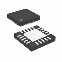
LTC6601IUF-1#PBF Linear Technology, LTC6601IUF-1#PBF Datasheet - Page 12

LTC6601IUF-1#PBF
Manufacturer Part Number
LTC6601IUF-1#PBF
Description
IC DRVR FILTER/ADC LN 20-QFN
Manufacturer
Linear Technology
Datasheet
1.LTC6601CUF-1PBF.pdf
(40 pages)
Specifications of LTC6601IUF-1#PBF
Frequency - Cutoff Or Center
28Mhz
Number Of Filters
3
Max-order
2nd
Voltage - Supply
2.7 V ~ 5.25 V
Mounting Type
Surface Mount
Package / Case
20-QFN
Lead Free Status / RoHS Status
Lead free / RoHS Compliant
Filter Type
-
Available stocks
Company
Part Number
Manufacturer
Quantity
Price
LTC6601-1
IN1
200Ω, 400Ω resistor which feeds a noninverting summing
node. Can accept an input signal, be fl oated or tied to OUT
For best performance, stray capacitance should be kept as
low as possible by keeping printed circuit connections as
short and direct as possible. If necessary, strip back the
surrounding ground plane away from these pins.
BIAS (Pin 3): Input to a three-state comparator whose
three states allow the user to tailor amplifi er power. The
pin impedance appears as a 150k resistor whose default
open-circuit potential is 1.15V with respect to the V
supply. If BIAS is driven to within 0.4V of the V
amplifi er is placed into a low power shutdown, consum-
ing typically 350μA. When BIAS is fl oated, the amplifi er
operates in its low power active state. Forcing the pin 2.3V
above V
state. See Applications Information for more detail.
IN1
200Ω, 400Ω resistor which feeds an inverting summing
node. Can accept an input signal, be fl oated or tied to
OUT
that stray capacitance be kept to as low as possible by
keeping printed circuit connections as short and direct
as possible, and if necessary, stripping back nearby sur-
rounding ground plane away from these pins.
C1, C2 (Pins 7, 8): Input to a trimmed 16.1pF , 33.3pF
capacitor which feeds a noninverting summing node.
Typically, either fl oat or tie to OUT
pins is tied to a low impedance source other than OUT
a resistance of at least 25Ω should be placed in series.
For best performance, it is highly recommended that stray
capacitance be kept to as low as possible by keeping printed
circuit connections as short and direct as possible, and
if necessary, stripping back nearby surrounding ground
plane away from these pins.
PIN FUNCTIONS
12
+
–
+
, IN2
, IN2
. For best performance, it is highly recommended
–
+
places the part into the high performance active
–
, IN4
, IN4
+
–
(Pins 2, 1, 20): Input to a trimmed 100Ω,
(Pins 4, 5, 6): Input to a trimmed 100Ω,
(Refer to the Block Diagram)
–
. If either of these
–
supply, the
–
power
–
–
.
,
C3, C4 (Pins 9, 10): Input to a trimmed 10.55pF , 21.1pF
capacitor which feeds the amplifi er inverting summing
node. Typically, either fl oat or tie to OUT
formance, it is highly recommended that stray capacitance
be kept to as low as possible by keeping printed circuit
connections as short and direct as possible, and if nec-
essary, stripping back nearby surrounding ground plane
away from these pins.
OUT
the internal feedback network, each pin can drive an ad-
ditional 50Ω to ground with typical short-circuit current
limiting of ±65mA. Capacitive loading of these pins should
be minimized by resistively decoupling the outputs from
the load with at least 25Ω.
V
The voltage on V
level (which is defi ned as the average of the voltages on
the OUT
of an internal resistive voltage divider between the sup-
plies, developing a (default) mid-supply voltage potential
to maximize output signal swing. The V
overdriven by an external voltage reference capable of
driving the input impedance presented by the V
The V
to a mid-supply potential. It should be bypassed with a
high quality ceramic bypass capacitor (for instance of X7R
dielectric) of at least 0.01μF , (unless using symmetrical
split supplies, then connect directly to a low impedance,
low noise ground plane) to minimize common mode noise
from being converted to differential noise by impedance
mismatches both externally and internally to the IC.
OCM
+
, OUT
OCM
(Pin 12): Output Common Mode Reference Voltage.
+
pin has an input resistance of approximately 18k
and OUT
–
(Pins 11, 15): Output Pins. Besides driving
OCM
–
sets the output common mode voltage
pins). The V
OCM
pin is the midpoint
OCM
+
. For best per-
pin can be
OCM
66011f
pin.


