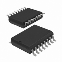
PCF8574AT/3,512 NXP Semiconductors, PCF8574AT/3,512 Datasheet - Page 21

PCF8574AT/3,512
Manufacturer Part Number
PCF8574AT/3,512
Description
IC I/O EXPANDER I2C 8B 16SOIC
Manufacturer
NXP Semiconductors
Datasheet
1.PCF8574ATS3118.pdf
(24 pages)
Specifications of PCF8574AT/3,512
Package / Case
16-SOIC (0.300", 7.5mm Width)
Interface
I²C
Number Of I /o
8
Interrupt Output
Yes
Frequency - Clock
100KHz
Voltage - Supply
2.5 V ~ 6 V
Operating Temperature
-40°C ~ 85°C
Mounting Type
Surface Mount
Includes
POR
Logic Family
PCF
Number Of Lines (input / Output)
9
Operating Supply Voltage
2.5 V to 6 V
Power Dissipation
400 mW
Operating Temperature Range
- 40 C to + 85 C
Maximum Clock Frequency
100 KHz
Mounting Style
SMD/SMT
Number Of Output Lines
9
Output Current
25 mA
Output Voltage
2.4 V
Lead Free Status / RoHS Status
Lead free / RoHS Compliant
For Use With
568-3615 - DEMO BOARD I2C
Lead Free Status / Rohs Status
Lead free / RoHS Compliant
Other names
568-3987-5
935275581512
PCF8574ATD
PCF8574ATD
935275581512
PCF8574ATD
PCF8574ATD
Philips Semiconductors
13.4
Notes
1. For more detailed information on the BGA packages refer to the “(LF)BGA Application Note ” (AN01026); order a copy
2. All surface mount (SMD) packages are moisture sensitive. Depending upon the moisture content, the maximum
3. For SDIP packages, the longitudinal axis must be parallel to the transport direction of the printed-circuit board.
4. These packages are not suitable for wave soldering. On versions with the heatsink on the bottom side, the solder
5. If wave soldering is considered, then the package must be placed at a 45 angle to the solder wave direction.
6. Wave soldering is suitable for LQFP, QFP and TQFP packages with a pitch (e) larger than 0.8 mm; it is definitely not
7. Wave soldering is suitable for SSOP and TSSOP packages with a pitch (e) equal to or larger than 0.65 mm; it is
2002 Nov 22
Through-hole mount DBS, DIP, HDIP, SDIP, SIL
Surface mount
Remote 8-bit I/O expander for I
from your Philips Semiconductors sales office.
temperature (with respect to time) and body size of the package, there is a risk that internal or external package
cracks may occur due to vaporization of the moisture in them (the so called popcorn effect). For details, refer to the
Drypack information in the “Data Handbook IC26; Integrated Circuit Packages; Section: Packing Methods” .
cannot penetrate between the printed-circuit board and the heatsink. On versions with the heatsink on the top side,
the solder might be deposited on the heatsink surface.
The package footprint must incorporate solder thieves downstream and at the side corners.
suitable for packages with a pitch (e) equal to or smaller than 0.65 mm.
definitely not suitable for packages with a pitch (e) equal to or smaller than 0.5 mm.
MOUNTING
Suitability of IC packages for wave, reflow and dipping soldering methods
BGA, LBGA, LFBGA, SQFP, TFBGA, VFBGA not suitable
HBCC, HBGA, HLQFP, HSQFP, HSOP,
HTQFP, HTSSOP, HVQFN, HVSON, SMS
PLCC
LQFP, QFP, TQFP
SSOP, TSSOP, VSO
(5)
, SO, SOJ
PACKAGE
2
(1)
C-bus
21
suitable
not suitable
suitable
not recommended
not recommended
(3)
WAVE
(4)
SOLDERING METHOD
(5)(6)
(7)
suitable
suitable
suitable
suitable
suitable
REFLOW
Product specification
PCF8574
(2)
DIPPING
suitable


