AMIS49587C5871RG ON Semiconductor, AMIS49587C5871RG Datasheet
AMIS49587C5871RG
Specifications of AMIS49587C5871RG
Available stocks


Related parts for AMIS49587C5871RG

AMIS49587C5871RG Summary of contents
Page 1
... AMIS- -49587 Product Preview Power Line Carrier Modem ON Semiconductor’s AMIS- -49587 is an IEC 61334- -5- -1 compliant power line carrier modem using spread- -FSK (S- -FSK) modulation for robust low data rate communication over power lines. AMIS- -49587 is built around an ARM 7TDMI processor core, and includes the MAC layer ...
Page 2
APPLICATION EXAMPLE NCS5650 1:2 MAINS Figure 1. Typical Application for the AMIS- -49587 S- -FSK Modem 1 APPLICATION 3V3_A TX_OUT TX _ENB RX_OUT RX_IN AMIS- -49587 REF_OUT ALC_IN 3V3_A M50HzIN http://onsemi.com 2 3V3_D T_REQ TXD Application RXD m Controller ...
Page 3
... Table 1. ORDERING INFORMATION Part No. Temperature Range AMIS49587C5871G --40°C -- +80°C AMIS49587C5871RG --40°C -- +80°C AMIS49587C5872G --40°C -- +80°C AMIS49587C5872RG --40°C -- +80°C †For information on tape and reel specifications, including part orientation and tape sizes, please refer to our Tape and Reel Packaging Specification Brochure, BRD8011/D. Table of Contents Application ...
Page 4
ABSOLUTE MAXIMUM RATINGS2.1 Stresses above those listed in this clause may cause permanent device failure. Exposure to absolute maximum ratings for extended periods may affect device reliability. 2.1.1 Power Supply Pins VDD, VDDA, VSS, VSSA Table 2. ABSOLUTE MAXIMUM ...
Page 5
PLCC Packaging M50Hz_IN RX_DATA Table 6. AMIS- -49587 PLCC PIN FUNCTION DESCRIPTION Pin No. Pin Name I/O 1 VSSA 2 RX_OUT Out 3 RX_IN In 4 REF_OUT Out 5 M50HZ_IN In 6 RX_DATA Out 7 TDO Out 8 TDI ...
Page 6
QFN Packaging M50Hz_IN RX _DATA Figure 3. QFN Pin- -out of AMIS- -49587 (Top view) Table 7. AMIS- -49587 QFN PIN FUNCTION DESCRIPTION Pin No. Pin Name I/O 1 M50HZ_IN In 6 RX_DATA Out 7 TDO Out 8 TDI ...
Page 7
Table 7. AMIS- -49587 QFN PIN FUNCTION DESCRIPTION Pin No. Pin Name I/O 37 TX_ENB Out 42 TX_OUT Out 43 ALC_IN In 46 VDDA 47 VSSA 48 RX_OUT Out 49 RX_IN In 51 REF_OUT Out 50, ...
Page 8
Figure 4. Recommended Layout of the Placement of Decoupling Capacitors for PLCC- -28 RX_OUT RX_OUT is the output analog pin of the receiver low noise input op- -amp. This op- -amp negative feedback configuration. RX_IN RX_IN is ...
Page 9
TDO, TDI, TCK, TMS, and TRSTB All these pins are part of the JTAG bus interface. The JTAG interface is used during production test of the IC and will not be described here. Input pins (TDI, TCK, TMS, and TRSTB) ...
Page 10
CRC CRC compliant open drain output. An external pull- -up resistor defines the logic high level as illustrated in Figure 5. A typical value for this pull- -up resistance “R” kΩ. The signal on this ...
Page 11
DC AND AC CHARACTERISTICS 4.1 4.1.1 Oscillator: Pin XIN, XOUT In production the actual oscillation of the oscillator and duty cycle will not be tested. The production test will be based on the static parameters and the inversion from XIN ...
Page 12
Transmitter External Parameters: Pin TX_OUT, ALC_IN, TX_ENB To guarantee the transmitter external specifications the TX_CLK frequency must be 12 MHz ± 100 ppm. Table 10. TRANSMITTER EXTERNAL PARAMETERS Parameter Maximum peak output level fTX_OUT = 23.75 kHz fTX_OUT = ...
Page 13
Receiver External Parameters: Pin RX_IN, RX_OUT, REF_OUT Table 12. RECEIVER EXTERNAL PARAMETERS: Pin RX_IN, RX_OUT, REF_OUT Parameter Input offset voltage 42 dB AGC gain = 42 dB Input offset voltage 0 dB AGC gain = 0 dB Max. peak ...
Page 14
Power- -on- -Reset (POR) Table 14. POWER- -ON- -RESET (POR) Parameter POR threshold Power supply rise time 4.1.6 Digital Outputs: TDO, CLK_OUT Table 15. DIGITAL OUTPUTS: TDO, CLK_OUT Parameter Low output voltage High output voltage 4.1.7 Digital Outputs with ...
Page 15
Current Consumption Table 20. CURRENT CONSUMPTION Parameter Current consumption in receive mode Current consumption in transmit mode Current consumption when RESB = 0 15. CLKARM is < 12 MHz, fCLK = 24 MHz. 4.1.12 Main Modem Characteristics Table 21. ...
Page 16
GENERAL DESCRIPTION 5.1 The AMIS- -49587 is a single chip half duplex S- -FSK modem dedicated to power line carrier (PLC) data transmission on low medium- -voltage power lines. The device offers complete handling of the protocol layers ...
Page 17
Test Mode: ♦ The Test Mode is used to test the compliance of a PLC modem conforms to CENELEC. EN 50065 Continuous broadcast ...
Page 18
IO handling. For most of the instructions, the machine is able to perform one instruction per clock cycle. The microcontroller contains the necessary hardware to implement interrupt mechanisms, timers and is able to perform byte multiplication over ...
Page 19
FROM MAINS 1 M Ω M50Hz_IN Figure 12. Zero Cross Detector with Falling Edge Debouncer The zero crossing detector output is logic zero when the input is lower than the falling threshold level and a logic one when the ...
Page 20
V MAINS VIR M 50HZIN ZeroCross CHIP _CLK *The start of the Physical Subframe is shifted back with R_ZC_ADJUST[7: Figure 14. Zero Cross Adjustment to Compensate for Zero Cross Delay (Example for 50 Hz) The ...
Page 21
Clock Generator and Timer The CHIP_CLK and f are used to generate a number CLK of timing signals used for the synchronization and interrupt generation. The timing generation has a fixed repetition rate which corresponds to the length of ...
Page 22
TRANSMITTER PATH DESCRIPTION (S- -FSK 6.2 MODULATOR) For the generation of the space and mark frequencies, the direct digital synthesis (DDS) of the sine wave signals is performed under the control of the microprocessor. After a signal conditioning step, a ...
Page 23
V output level. When switching between f accumulator must give a continuous phase and not restart from phase 0. When AMIS- -49587 goes into receive mode (when TX_RXB goes ...
Page 24
R_ALC_CTRL[2:0]. See WriteConfigRequest. Table 25. FIXED TRANSMITTER OUTPUT ATTENUATION ALC_CTRL[2:0] 000 001 010 011 100 101 110 111 Remark: The analog part of AMIS- -49587 works with an analogue ...
Page 25
Hz Suppression Filter AMIS- -49587 receiver input provides a low noise input operational amplifier in a follower configuration which can be used to make a 50/60 Hz suppression filter with Received Signal C ...
Page 26
Table 26. VALUE OF THE RESISTORS AND CAPACITORS Component Value DREF Remark: The analog part of AMIS- -49587 is referenced to the internal analog ground REF_OUT ...
Page 27
Communication Controller Data RAM Program ROM Timer 1 & TRANSMIT FROM RECEIVER Interrupt Control 6.4.1 Local Port The controller uses 3 output ports to inform the actual status of the PLC communication. RX_DATA indicates if AMIS- -49587 is ...
Page 28
Table 27. OVERVIEW FUNCTIONALITY LOCAL PORT Port Function RX_DATA Data reception CRC CRC OK TX_DATA / TX_DATA PRE_SLOT PRE_SLOT 6.4.2 Serial Communication Interface (SCI) The Serial Communication asynchronous communication. It can communicate with a UART = Universal Asynchronous Receiver Transmitter, ...
Page 29
Serial Communication Interface Physical Layer Description The following pins control the serial communication interface. TXD: Transmit data output the data output of the AMIS- -49587 and the input of the application micro controller. RXD: Receive data input. ...
Page 30
T_REQ t POLL TxD Status Message RxD Figure 26. Transfer from Application Microcontroller to AMIS- -49587 If the length and the checksum of the local frame are both correct, the AMIS- -49587 acknowledges with an <ACK> character. In other cases, ...
Page 31
After this delay, the frame reception is finished. If the length and the checksum are both correct, the local frame is taken in account otherwise all previous characters are discarded. The time out Inter Character ( after ...
Page 32
MAINS_FREQ R_FS and R_FM step registers are defining the space and mark frequency. Explanation on the values can be found in paragraph Sine wave generator. This register can be accessed via a WriteConfig_Request. Table 31. FS AND ...
Page 33
Figure 29 depicts a typical PLC network with one master and 2 slaves. Each AMIS- -49587 is controlled by an external CPU over a RS232 interface. See paragraph Serial Communication Interface Physical Layer Description for a description on hardware signals ...
Page 34
Table 36. Field Byte Length START 1 Status_Data 4 Important: Frame in little endian format (LSByte first) STATUS MESSAGE IN NOT SET MODE Bit 7 Byte Content 1 Start 0 2 Data Data 2 4 Data 3 ...
Page 35
Status Message in MASTER or CLIENT MODE: STATUS MESSAGE IN SLAVE MODE Bit 7 Byte Content 1 Start 0 2 Data Data 2 4 Data 3 Where: Not SYNC Indication of synchronization with mains Not SET ...
Page 36
Table 38. Field Byte Length <STX> 1 Length 1 Command 1 User_Data 0 .. 247 CHK 2 Important: Frame in little endian format (LSByte first) Table 39. SUMMARY OF FRAME DELIMITERS Character <STX> Start of text; first char of frame ...
Page 37
Table 40. CONFIGURATION COMMANDS AND RESPONSES Command Unsolicited* Reset_Request WriteConfig_Request WriteConfig_Confirm WriteConfig_Error AccessDB_Request AccessDB_Confirm AccessDB_Error *An unsolicited message is a message that is originating from the AMIS--49587, based upon an AMIS--49587 internal event. The message is not provoked by a ...
Page 38
WriteConfig_Request External CPU WriteConfigNew _Request(0x71) [Config data error| Command not allowed| Test mode] [Config data OK&& Command allowed&& !Test mode] WriteConfigNew _Confirm (0x72) Figure 32. Sequence Diagram for WriteConfig_Request Command can be issued at any time (If the status ...
Page 39
Table 41. CONFIGURATION PARAMETERS Field NbAlarm R_ALC_CTRL→Value Max_Transmitting_Gain→Value R_ALC_CTRL→Value Max_Transmitting_Gain→Mode R_CONF_TX_DATA_PRE_SLOT_SEL Pad R_CONF→MODE R_CONF→BAUDRATE R_CONF→MAINS_FREQ Pad Search method SINC Filter SYNCHRO--Type→Mode SYNCHRO--Bit→Value SYNCHRO--Bit→Mode SearchInitiatorGain or Min--ReceivingGain Mode Search Initiator Gain or Min--Receiving Gain Max--Receiving--Gain→Value Max--Receiving--Gain→Mode Time out Inter Character TIC ...
Page 40
Table 41. CONFIGURATION PARAMETERS Field Pad correcting FSK + Synchro Master Synchro without Gain Min Repeater Time--out--search--initiator 23. When a time--out is written with a 0x0000 value using either the WriteConfig_Request or the AccessDB_Request command, this time--out will not be ...
Page 41
Table 42. NON CHANGEABLE PARAMETERS AFTER AMIS 49587 IS SET Field R_CONF_TX_DATA_PRE_SLOT_SEL R_CONF→MODE R_CONF→BAUDRATE R_CONF→MAINS_FREQ Table 43. WriteConfig ERROR CODES Error Identifier ERR_UNAVAILABLE_MODE ERR_ILLEGAL_DATA_COMMAND ERR_ILLEGAL_LOCAL_MAC_ADR ERR_ILLEGAL_INITIATOR_MAC_ADR ERR_UNAVAILABLE_COMMAND 7.3.5 AccessDB_Request External CPU Figure 33. Sequence Diagram for AccessDB_Request <STX> 0x07 + ...
Page 42
Table 44. DATA BASE ENTRIES THAT MODIFY THE CONFIGURATION Field Name FIMA/LIMA LocalMacAdd/InitMacAdd Time--out--synchro--confirm Time--out--frame--not--ok Time--out--not--addressed Mac--group--addresses Min--delta--credit Max_Transmitting_Gain: Mode and Value (R_ALC_CTRL) SYNCHRO--Type:Mode SYNCHRO--Bit:Value Max--Receiving--Gain: Mode and Value Repeater Frequency Time--SearchInitiator ReadConfig Read SoftVersion Min--ReceivingGain Value Gain--SearchInitiator 7.3.5.1 FIMA/LIMA ...
Page 43
Confirm Format: <STX> 0x07(Length) 0x42 (AccessDB_Confirm) 7.3.5.4 TimeoutNotOK This request is used to modify the value of the timeout Frame Not OK. The Timeout Frame Not OK is set in seconds. Request Format: <STX> 0x07(Length) 0x41 (AccessDB_Request) Confirm Format: <STX> ...
Page 44
MaxReceivingGain This request is used to modify the Max Receiving Gain of the AMIS- -49587. The Max Receiving Gain can be set from step of step 6 dB, or unlimited. The data value for ...
Page 45
Confirm Format: <STX> 0x06(Length) 0x42 (AccessDB_Confirm) 7.3.5.15 Min- ReceivingGain This request is used to modify the Min Receiving Gain of the AMIS- -49587. The Min Receiving Gain can be set from step of step 6 ...
Page 46
SEND AND RECEIVE NETWORK DATA WITH 7.4 THE AMIS- -49587 The data path should be implemented like specified in IEC 61334- -5- -1. The MAC layer is implemented by the AMIS- -49587, the LLC layer should be implemented by the ...
Page 47
MA_DATA_Indication External CPU MA_DATA_Indicator(0x50) Figure 35. Sequence Diagram for MA_DATA_Indication The MA_Data_Indication is sent from the AMIS- -49587 (Client or Server) to the external controller to deliver the received DLC frame. Frame Format: <STX> Length 7.4.2 MA_DATA_Request External CPU ...
Page 48
Table 47. DESCRIPTION OF THE MAC_Frame FIELD Field Name Length Initial Credit 3 bits b7--b5 Current Credit 3 bits b4--b2 Delta Credit 2 bits b1,b0 Source Address 12 bits b23--b12 Destination Address 12 bits b11--b0 Pad length 1 byte M_sdu ...
Page 49
Table 49. DESCRIPTION OF THE SpyData FIELD Field Name Length S0 2 Bytes N0 2 Bytes S1 2 Bytes N1 2 Bytes Threshold 2 Bytes Method 1 Byte PAD 1 Bit (b7) Synchro_bit Value 3 Bits (b6,b5,b4) PAD 1 Bit ...
Page 50
Spy_No_Alarm_Found The SPY_Alarm_Found is sent by the AMIS- -49587 local MAC sub- -layer as soon as it has correctly found a Alarm indication in the pause time. For the format of the SpyData field, see Table 49. The AlarmPattern ...
Page 51
The Synchro_Data field contains a synchronization event description bytes with accompanying data. Table 50. Synchro_Data FIELDS Event Description, byte 1 Event Description, byte 2 0x01 Synchronization Found 0x02 Synchronization Confirmed 0x04 Synchronization Lost Time--out not addressed ...
Page 52
PhyAlarmRequest Description: This request is used to send a physical alarm pattern. No data is transmitted to indicate the number of repetitions, the AMIS- -49587 already knows this number because its set of configuration data. Request ...
Page 53
Data Counters The Data Counters request is used to read the value of the data counters in the AMIS- -49587. It contains one byte which is used to know whether the counters must be reset or not (00: no ...
Page 54
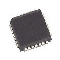
PACKAGE DIMENSIONS PLCC 28 LEAD CASE 776AA--01 ISSUE O http://onsemi.com 54 ...
Page 55
... Equal Opportunity/Affirmative Action Employer. This literature is subject to all applicable copyright laws and is not for resale in any manner. PUBLICATION ORDERING INFORMATION LITERATURE FULFILLMENT: Literature Distribution Center for ON Semiconductor P.O. Box 5163, Denver, Colorado 80217 USA Phone: 303--675--2175 or 800--344--3860 Toll Free USA/Canada Fax: 303--675--2176 or 800--344--3867 Toll Free USA/Canada Email: orderlit@onsemi ...