AD693AD Analog Devices Inc, AD693AD Datasheet
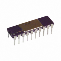
IC SGNL COND 4-20MA TX 20-CDIP

AD693AD

Manufacturer Part Number
AD693AD
Description
IC SGNL COND 4-20MA TX 20-CDIP
Manufacturer
Analog Devices Inc
Type
Signal Conditionerr
Datasheet

Specifications of AD693AD

Rohs Status
RoHS non-compliant
Input Type
Voltage
Output Type
Voltage
Interface
3-Wire
Current - Supply
20mA
Mounting Type
Through Hole
Package / Case
20-CDIP (0.300", 7.62mm)
No. Of Amplifiers
5
Input Offset Voltage
200µV
Cmrr
90dB
Supply Voltage Range
12V To 36V
Supply Current
500µA
Amplifier Case Style
DIP
No. Of Pins
20
Operating Temperature Range
-40°C To +85°C
Rohs Compliant
No

Available stocks

Company
Part Number
Manufacturer
Quantity
Price
Part Number:
AD693AD
Manufacturer:
ADI/亚德诺
Quantity:
20 000
a
REV. A
Information furnished by Analog Devices is believed to be accurate and
reliable. However, no responsibility is assumed by Analog Devices for its
use, nor for any infringements of patents or other rights of third parties
which may result from its use. No license is granted by implication or
otherwise under any patent or patent rights of Analog Devices.
PRODUCT DESCRIPTION
The AD693 is a monolithic signal conditioning circuit which
accepts low-level inputs from a variety of transducers to control a
standard 4–20 mA, two-wire current loop. An on-chip voltage
reference and auxiliary amplifier are provided for transducer
excitation; up to 3.5 mA of excitation current is available when the
device is operated in the loop-powered mode. Alternatively, the
device may be locally powered for three-wire applications when
0–20 mA operation is desired.
Precalibrated 30 mV and 60 mV input spans may be set by
simple pin strapping. Other spans from 1 mV to 100 mV may
be realized with the addition of external resistors. The auxiliary
amplifier may be used in combination with on-chip voltages to
provide six precalibrated ranges for 100
and zero are also determined by pin strapping to obtain the
standard ranges: 4–20mA, 12
Active laser trimming of the AD693’s thin-film resistors result
in high levels of accuracy without the need for additional
adjustments and calibration. Total unadjusted error is tested on
every device to be less than 0.5% of full scale at +25 C, and less
than 0.75% over the industrial temperature range. Residual
nonlinearity is under 0.05%. The AD693 also allows for the use
of an external pass transistor to further reduce errors caused by
self-heating.
For transmission of low-level signals from RTDs, bridges and
pressure transducers, the AD693 offers a cost-effective signal
conditioning solution. It is recommended as a replacement for
discrete designs in a variety of applications in process control,
factory automation and system monitoring.
The AD693 is packaged in a 20-pin ceramic side-brazed DIP,
20-pin Cerdip, and 20-pin LCCC and is specified over the
–40 C to +85 C industrial temperature range.
FEATURES
Instrumentation Amplifier Front End
Loop-Powered Operation
Precalibrated 30 mV or 60 mV Input Spans
Independently Adjustable Output Span and Zero
Precalibrated Output Spans: 4–20 mA Unipolar
Precalibrated 100
6.2 V Reference with Up to 3.5 mA of Current Available
Uncommitted Auxiliary Amp for Extra Flexibility
Optional External Pass Transistor to Reduce
Self-Heating Errors
RTD Interface
8 mA and 0–20 mA.
0–20 mA Unipolar
12
8 mA Bipolar
RTDs. Output span
PRODUCT HIGHLIGHTS
10. Six precalibrated temperature ranges are available with a
One Technology Way, P.O. Box 9106, Norwood, MA 02062-9106, U.S.A.
Tel: 617/329-4700
1. The AD693 is a complete monolithic low-level voltage-to-
2. Precalibrated output zero and span options include
3. Simple resistor programming adds a continuum of ranges
4. The common-mode range of the signal amplifier input
5. Provision for transducer excitation includes a 6.2 V
6. The circuit configuration permits simple linearization of
7. A monitored output is provided to drive an external pass
8. Laser-wafer trimming results in low unadjusted errors and
9. Zero and span are independently adjustable and noninteractive
current loop signal conditioner.
4–20 mA, 0–20 mA, and 12
configurations.
to the basic 30 mV and 60 mV input spans.
extends from ground to near the device’s operating voltage.
reference output and an auxiliary amplifier which may be
configured for voltage or current output and signal
amplification.
bridge, RTD, and other transducer signals.
transistor. This feature off-loads power dissipation to
extend the temperature range of operation, enhance
reliability, and minimize self-heating errors.
affords precalibrated input and output spans.
to accommodate transducers or user defined ranges.
100
RTD via pin strapping.
FUNCTIONAL BLOCK DIAGRAM
Loop-Powered 4–20 mA
Sensor Transmitter
8 mA in two- and three-wire
AD693
Fax: 617/326-8703

Related parts for AD693AD

AD693AD Summary of contents

Page 1

FEATURES Instrumentation Amplifier Front End Loop-Powered Operation Precalibrated Input Spans Independently Adjustable Output Span and Zero Precalibrated Output Spans: 4–20 mA Unipolar 0–20 mA Unipolar 12 Precalibrated 100 RTD Interface 6.2 V Reference with ...

Page 2

... Input Span 60 mV Input Span Into Pin 6 Output Span = 4– REF Loop Powered, (Figure 10) 3-Wire Mode, (Figure 15) –2– AD693AD/AQ/AE Min Typ Max Units 0.25 0.5 % Full Scale 0.4 0.75 % Full Scale 0.5 2 120 +7 +35 +100 0.5 1.5 3.0 5 – ...

Page 3

... AD693AQ Cerdip AD693AE Leadless Ceramic Chip Carrier (LCCC) REV. A Conditions Pin I OUT X Pin V – Pin MIN MAX RTD at 0 and +100 Package Option D-20 Q-20 E-20A –3– AD693AD Min Typ Max Units – 200 +5 +20 nA +0.5 3 105 dB +0. 0.005 % –40 +85 C – ...

Page 4

AD693–Typical Characteristics Figure 1. Maximum Load Resistance vs. Power Supply Figure 2. Differential Input Current vs. Input Signal Voltage Normalized to +IN Figure 3. Maximum Common-Mode Voltage vs. Supply Figure 4. Bandwidth vs. Series Load Resistance Figure 5. Signal Amplifier ...

Page 5

FUNCTIONAL DESCRIPTION The operation of the AD693 can be understood by dividing the circuit into three functional parts (see Figure 9). First, an instrumentation amplifier front-end buffers and scales the low- level input signal. This amplifier drives the second section, ...

Page 6

AD693 if the 6 the reference is unsuitable. Configured as a simple follower, it can be driven from a user supplied voltage divider or the precalibrated outputs of the AD693 divider (Pins 3 and 4) to provide a ...

Page 7

Figure 11. Using an External Pass Transistor to Minimize Self-Heating Errors of adjustment of the output current from nominal. Substitute this value in the appropriate formula below for adjustment at the 4 mA tap (1.6 V/I ) – ...

Page 8

AD693 An alternative arrangement, allowing wide range span adjust- ment between two set ranges, is shown in Figure 13 are calculated to be 90% of the values determined from the S2 previous formulae. The smallest value is then ...

Page 9

Figure 15. Local Powered Operation with 0–20 mA Output OPTIONAL INPUT FILTERING Input filtering is recommended for all applications of the AD693 due to its low input signal range filter network at each input of the signal amplifier ...

Page 10

AD693 increasing the application voltages by adding resistance between Pins 14 and 3 will decrease the temperature span. An external voltage divider may also be used in conjunction with the circuit shown to produce any range of temperature spans as ...

Page 11

Figure 19. Thermocouple Inputs with Cold Junction Compensation Table II. Thermocouple Application—Cold Junction Compensation POLARITY MATERIAL + IRON – CONSTANTAN + NICKEL-CHROME _ NICKEL-ALUMINUM + NICKEL-CHROME – COPPER-NICKEL + COPPER – COPPER-NICKEL via a set of thermocouple tables referenced to ...

Page 12

AD693 and an input common-mode voltage of 3.1 V. The expressions below calculate errors due to deviations from these nominal conditions. The total error at zero consists only of offset errors. The total error at full scale consists of the ...

Related keywords