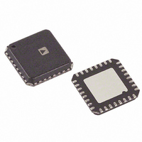
AD9943KCPZ Analog Devices Inc, AD9943KCPZ Datasheet

AD9943KCPZ
Specifications of AD9943KCPZ
Available stocks
Related parts for AD9943KCPZ
AD9943KCPZ Summary of contents
Page 1
FEATURES 25 MSPS correlated double sampler (CDS 10-bit variable gain amplifier (VGA) Low noise optical black clamp circuit Preblanking function 10-bit (AD9943), 12-bit (AD9944) 25 MSPS A/D converter No missing codes guaranteed 3-wire serial digital ...
Page 2
AD9943/AD9944 TABLE OF CONTENTS AD9943/AD9944 Specifications..................................................... 3 General Specifications ................................................................. 3 Digital Specifications ................................................................... 3 AD9943 System Specifications ....................................................... 4 AD9944 System Specifications ....................................................... 5 Timing Specifications....................................................................... 6 Absolute Maximum Ratings............................................................ 7 Thermal Characteristics .............................................................. 7 ESD Caution.................................................................................. 7 AD9943 ...
Page 3
AD9943/AD9944 SPECIFICATIONS GENERAL SPECIFICATIONS AVDD = DVDD = DRVDD = MIN MAX Table 1. Parameter TEMPERATURE RANGE Operating Storage POWER SUPPLY VOLTAGE Analog, Digital, Digital Driver POWER CONSUMPTION Normal Operation Power-Down Mode MAXIMUM ...
Page 4
AD9943/AD9944 AD9943 SYSTEM SPECIFICATIONS AVDD = DVDD = DRVDD = MIN MAX Table 3. Parameter CDS Maximum Input Range before Saturation Allowable CCD Reset Transient 1 Maximum CCD Black Pixel Amplitude VARIABLE GAIN ...
Page 5
AD9944 SYSTEM SPECIFICATIONS AVDD = DVDD = DRVDD = MIN MAX Table 4. Parameter CDS Maximum Input Range before Saturation Allowable CCD Reset Transient 1 Maximum CCD Black Pixel Amplitude 1 VARIABLE GAIN ...
Page 6
AD9943/AD9944 TIMING SPECIFICATIONS pF MHz. See CCD-mode timing in Figure 14 and Figure 15, and serial timing in Figure 10 and Figure 11. L SAMP Table 5. Parameter SAMPLE CLOCKS DATACLK, SHP, SHD Clock ...
Page 7
ABSOLUTE MAXIMUM RATINGS Table 6. Parameter (With Respect To) Min AVDD (AVSS) −0.3 DVDD (DVSS) −0.3 DRVDD (DRVSS) −0.3 Digital Outputs (DRVSS) −0.3 SHP, SHD, DATACLK (DVSS) −0.3 CLPOB, PBLK (DVSS) −0.3 SCK, SL, SDATA DVSS (AVSS) −0.3 REFT, REFB, ...
Page 8
AD9943/AD9944 AD9943 PIN CONFIGURATION AND FUNCTION DESCRIPTIONS Table 7. AD9943 Pin Function Descriptions Pin No. Mnemonic Type DRVDD P 12 DRVSS P 13 DVDD P 14 DATACLK DI 15 DVSS P 16 ...
Page 9
AD9944 PIN CONFIGURATION AND FUNCTION DESCRIPTIONS Table 8. AD9944 Pin Function Descriptions Pin No. Mnemonic Type D11 DO 11 DRVDD P 12 DRVSS P 13 DVDD P 14 DATACLK DI 15 DVSS P 16 PBLK ...
Page 10
AD9943/AD9944 TERMINOLOGY Differential Nonlinearity (DNL) An ideal ADC exhibits code transitions that are exactly 1 LSB apart. DNL is the deviation from this ideal value. Therefore every code must have a finite width. No missing codes guaranteed to 10-bit resolution ...
Page 11
EQUIVALENT INPUT CIRCUITS DVDD 330Ω INPUT DVSS Figure 4. Digital Inputs—SHP, SHD, DATACLK, CLOB, PBLK, SCK, SL DVDD DATA THREE- STATE DVSS Figure 5. Data Outputs DRVDD DOUT DRVSS Rev Page AD9943/AD9944 AVDD 60Ω AVSS ...
Page 12
AD9943/AD9944 TYPICAL PERFORMANCE CHARACTERISTICS 100 SAMPLE RATE (MHz) Figure 7. AD9943/AD9944 Power vs. Sample Rate 0.50 0.25 0 –0.25 –0.50 ...
Page 13
INTERNAL REGISTER MAP All register values default to 0x000 at power-up except clamp level, which defaults to 128 decimal (AD9943 = 32 LSB clamp level, and AD9944 = 128 LSB clamp level). Table 9. Address Bits Register Name A2 A1 ...
Page 14
AD9943/AD9944 SERIAL INTERFACE SDATA SCK NOTES 1. SDATA BITS ARE INTERNALLY LATCHED ON THE RISING EDGES OF SCK. 2. SYSTEM UPDATE OF LOADED REGISTERS OCCURS ON SL RISING EDGE. 3. ...
Page 15
CIRCUIT DESCRIPTION AND OPERATION DC RESTORE 0.1µF CCDIN The AD9943/AD9944 signal processing chain is shown in Figure 12. Each processing step is essential for achieving a high quality image from the raw CCD pixel data. DC RESTORE To reduce the ...
Page 16
AD9943/AD9944 A/D CONVERTER The ADC uses input range. Better noise performance results from using a larger ADC full-scale range. The ADC uses a pipelined architecture with full-scale input for low noise performance. VARIABLE GAIN ...
Page 17
CCD MODE TIMING CCD SIGNAL SHP t S1 SHD DATACLK t OD OUTPUT N – 10 DATA NOTES 1. RECOMMENDED PLACEMENT FOR DATACLK RISING EDGE IS BETWEEN THE SHD RISING EDGE AND NEXT SHP FALLING ...
Page 18
AD9943/AD9944 APPLICATIONS INFORMATION The AD9943/AD9944 are complete analog front end (AFE) products for digital still camera and camcorder applications. As shown in Figure 12, the CCD image (pixel) data is buffered and sent to the AD9943/AD9944 analog input through a ...
Page 19
DATA OUTPUTS CONNECT INTERNAL POWER-ON RESET CIRCUITRY After power-on, the AD9943/AD9944 automatically reset all internal registers and perform internal calibration procedures. This takes approximately complete. During this time, normal clock signals and serial ...
Page 20
... Temperature Range −20°C to +85°C AD9943KCP −20°C to +85°C AD9943KCPRL −20°C to +85°C 1 AD9943KCPZ −20°C to +85°C 1 AD9943KCPZRL −20°C to +85°C AD9944KCP −20°C to +85°C AD9944KCPRL −20°C to +85°C AD9944KCPZ 1 −20°C to +85°C 1 ...


