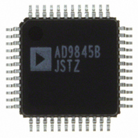
AD9845BJSTZ Analog Devices Inc, AD9845BJSTZ Datasheet

AD9845BJSTZ
Specifications of AD9845BJSTZ
Available stocks
Related parts for AD9845BJSTZ
AD9845BJSTZ Summary of contents
Page 1
FEATURES Pin Compatible with AD9845A Designs 12-Bit 30 MSPS A/D Converter 30 MSPS Correlated Double Sampler (CDS 6-Bit Pixel Gain Amplifier ( PxGA 10-Bit Variable Gain Amplifier (VGA) Low Noise Clamp ...
Page 2
AD9845B–SPECIFICATIONS GENERAL SPECIFICATIONS Parameter TEMPERATURE RANGE Operating Storage POWER SUPPLY VOLTAGE Analog, Digital, Digital Driver POWER CONSUMPTION Normal Operation Power-Down Modes Standby Total Power-Down MAXIMUM CLOCK RATE A/D CONVERTER Resolution Differential Nonlinearity (DNL) No Missing Codes Full-Scale Input Voltage Data ...
Page 3
CCD MODE SPECIFICATIONS Parameter P OWER CONSUMPTION MAXIMUM CLOCK RATE CDS Gain 1 Allowable CCD Reset Transient 1 Max Input Range before Saturation 1 Max CCD Black Pixel Amplitude PIXEL GAIN AMPLIFIER (PxGA) Max Input Range Max Output Range Gain ...
Page 4
AD9845B AUX1 MODE SPECIFICATIONS Parameter POWER CONSUMPTION MAXIMUM CLOCK RATE INPUT BUFFER Gain Max Input Range VGA Max Output Range Gain Control Resolution Gain (Selected Using VGA Gain Register) Min Gain Max Gain Specifications subject to change without notice. AUX2 ...
Page 5
TIMING SPECIFICATIONS Serial Timing in Figures 21–24.) Parameter SAMPLE CLOCKS DATACLK, SHP, SHD Clock Period DATACLK High/Low Pulsewidth SHP Pulsewidth SHD Pulsewidth CLPDM Pulsewidth CLPOB Pulsewidth * SHP Rising Edge to SHD Falling Edge SHP Rising Edge to SHD ...
Page 6
AD9845B Pin Number Name 1–12 D0–D11 13 DRVDD 14 DRVSS 15, 41 DVSS 16 DATACLK 17 DVDD1 PBLK 20 CLPOB 21 SHP 22 SHD 23 CLPDM 24 VD 25, 26, 35 AVSS 27 AVDD1 28 BYP1 29 ...
Page 7
DEFINITIONS OF SPECIFICATIONS Differential Nonlinearity (DNL) An ideal ADC exhibits code transitions that are exactly 1 LSB apart. DNL is the deviation from this ideal value. Thus, every code must have a finite width. No missing codes guaranteed to 12-bit ...
Page 8
AD9845B–Typical Performance Characteristics 190 180 170 V = 3.3V DD 160 150 V = 3.0V DD 140 130 V = 2.7V DD 120 110 100 0 20 SAMPLE RATE – MHz TPC 1. Power vs. Sample Rate 0.5 0.25 0 ...
Page 9
CCD MODE AND AUX MODE TIMING CCD SIGNAL SHP t S1 SHD t INH DATACLK t OD OUTPUT N–10 DATA NOTES 1. RECOMMENDED PLACEMENT FOR DATACLK RISING EDGE IS BETWEEN THE SHD RISING EDGE AND ...
Page 10
AD9845B PIXEL GAIN AMPLIFIER (PxGA) TIMING FRAME N VD 0101... 2323... LINE 0 LINE GAIN0 GAIN1 GAIN2 GAIN3 Figure 8. PxGA Mode 1 (Mosaic Separate) Frame/Line Gain Register Sequence 5 ...
Page 11
VD 012012012... GAIN0 GAIN1 GAIN2 Figure 12. PxGA Mode 3 (3-Color) Frame/Line Gain Register Sequence 5 PIXEL MIN VD 5 PIXEL MIN HD SHP PxGA GAIN NOTES 1. BOTH VD AND HD ARE ...
Page 12
AD9845B VD EVEN FIELD 0101... 0101... 0101... LINE 0 LINE 1 LINE GAIN0 GAIN1 GAIN2 GAIN3 Figure 16. PxGA Mode 5 (VD Selected) Frame/Line Gain Register Sequence VD 5 PIXEL ...
Page 13
VD HD 3ns MIN SHP PxGA GAIN GAIN0 NOTES 1. BOTH VD AND HD ARE INTERNALLY UPDATED AT SHP RISING EDGES AND SELECTS GAIN0 AND SELECTS ...
Page 14
AD9845B SERIAL INTERFACE TIMING AND INTERNAL REGISTER DESCRIPTION Register Address Name Operation Channel Select Power-Down CCD/AUX1/2 Modes VGA Gain LSB Clamp Level LSB Control ...
Page 15
BITS OPERATION RNW SDATA SCK NOTES 1. ANY NUMBER OF ADJACENT REGISTERS MAY BE LOADED SEQUENTIALLY, BEGINNING WITH THE LOWEST ADDRESS AND INCREMENTING ...
Page 16
AD9845B Table IV. Clamp Level Register Contents (Default Value x080) MSB D10 Table V. Control Register Contents (Default Value x000) Data Out DATACLK D10 ...
Page 17
CIRCUIT DESCRIPTION AND OPERATION The AD9845B signal processing chain is shown in Figure 25. Each processing step is essential in achieving a high quality image from the raw CCD pixel data. DC Restore To reduce the large dc offset of ...
Page 18
AD9845B MOSAIC SEPARATE COLOR CCD: PROGRESSIVE BAYER STEERING MODE Gr LINE0 GAIN0, GAIN1, GAIN0, GAIN1... LINE1 GAIN2, GAIN3, GAIN2, GAIN3... LINE2 GAIN0, GAIN1, GAIN0, GAIN1... ...
Page 19
A/D Converter The AD9845B uses high performance ADC architecture, opti- mized for high speed and low power. Differential ...
Page 20
AD9845B APPLICATIONS INFORMATION The AD9845B is a complete analog front end (AFE) product for digital still camera and camcorder applications. As shown in Figure 32, the CCD image (pixel) data is buffered and sent to the AD9845B analog input through ...
Page 21
SERIAL INTERFACE (MSB) D11 12 DATA OUTPUTS DRIVER SUPPLY Figure 33. Recommended Circuit Configuration for CCD-Mode Internal Power-On Reset Circuitry After power-on, the AD9845B will automatically reset all inter- nal registers and perform internal calibration procedures. This takes approximately 1 ...
Page 22
AD9845B 1.45 1.40 1.35 0.15 SEATING 0.05 PLANE ROTATED 90 CCW OUTLINE DIMENSIONS 48-Lead Plasitc Quad Flatpack [LQFP] 1.4 mm Thick (ST-48) Dimensions shown in millimeters 1.60 MAX PIN 1 INDICATOR 0.75 0.60 0.45 SEATING PLANE 0.20 0.09 VIEW A ...
Page 23
–23– ...
Page 24
–24– ...


